Back in May I wrote a post explaining the architecture of AMD NPUs and demonstrating a simple kernel that reaches close to the peak TOPS allowed by the hardware resources. That program was very simple and there was no data movement between the NPU compute tiles and the rest of the system. After writing that post, I wanted to write a more complex program to understand better the NPU architecture and the software stack, and what the challenges are when working on real-world projects.
I decided to implement an X-engine correlator, such as the ones commonly used in radio astronomy. This is a problem that I’m personally interested in, and it is basically a big matrix multiplication, with some small caveats that I will explain below. As the main goal of NPUs is to be used for matrix multiplication in machine learning inference, I thought “how hard can this be?”. After a few months of working on and off on this project, I now have something ready to show.
The design has actually been quite challenging. There are many nuances I will get into below, and many dead-end paths I have taken until I discovered that when using some particular approaches performance would be killed for one reason or another, so I had to backtrack multiple times. I should also mention that while it is usually very clear what is happening at low level (which was one of the main messages of my previous post), the lack of flexibility of the hardware is often quite limiting, in particular regarding the programmability of the DMA engines, so it is quite challenging to design approaches that actually work well in the hardware.
This post is a full presentation of my X-engine implementation.
X-engine primer
Correlators are used in radio astronomy and similar applications involving antenna arrays to compute the matrix of cross-correlations between all the antenna pairs (baselines) of the array (in more technical terms, the spatial covariance matrix). The output of a correlator is often used for imaging in radio astronomy, but it can be used for angle-of-arrival estimation in other applications. The main case I will have in mind is an array of dishes (which have a relatively narrow field of view) in radio astronomy, but the X-engine designed here can be applied to other use cases, perhaps with minor modifications.
The most common correlator architecture in radio astronomy is called FX. This architecture is formed by an F-engine for each antenna followed by an X-engine that puts together the data of all the antennas. The F-engine is a channelizer, usually a polyphase filterbank or a simple FFT. There are three reasons to apply a channelizer at this stage, which set the requirements for this channelizer:
- In order to implement cross-correlation as multiplication in the frequency domain, a channelizer is used first to pass to the frequency domain. Typically, delays are applied to the sample streams of each antenna before channelization in order to align the streams as well as possible taking into account geometric delays given by the source location and instrumental delays. Any residual delays (which can simply happen because of errors in the calibration or because of sources having different geometric delays, which is a major factor if the field of view of the array is large) will show up as delays in the correlation outputs. Therefore, the channel width needs to be much smaller than the inverse of the residual delays to avoid correlation losses caused by FFTs overlapping only partially.
- Typically, frequency-dependent gain and phase calibration of instrumental effects at each antenna needs to be applied. It is simpler to perform these calibrations as a multiplication by a complex scalar on each channel, rather than as convolution in the time domain with an appropriate filter. These per-channel calibrations can even be applied at the correlator output in many cases. The channel width needs to be smaller than the scale with which these calibrations vary in the frequency domain, so that the calibration to apply within each channel is roughly a constant with respect to frequency.
- It is often impossible to perform the cross-correlation of all the antennas and all the frequency spectrum in a single machine. The workload can be easily split and parallelized by giving different frequency chunks to different machines. This is trivial to do if the data is channelized, since it is just a matter of distributing blocks of channels to each machine. This is usually the least stringent requirement regarding channel width, since machines are often capable of processing many 10s of MHz of spectrum, or even a few 100 MHz, while the other requirements typically set a channel width on the order of 1 MHz (and even much narrower for all-sky low frequency arrays).
The X-engine works independently on each channel output by the F-engines. It takes all the antenna pairs, forms their complex-conjugate products, and integrates coherently over time in order to produce an output. In formula, if we denote by \(x_{j,c}[n]\) the F-engine output corresponding to antenna \(j\), channel \(c\), and time index \(n\) (this output is a complex number), and by \(T\) the integration time in samples, the X-engine computes\[y_{j,k,c}[m] = \sum_{n = 0}^{T-1} x_{j,c}[n+Tm]\overline{x_{k,c}[n+Tm]}.\]This operation can be written as a matrix product. If we form the \(S \times T\) matrix\[A_{c,m} = \begin{pmatrix}x_{0,c}[mT] & x_{0,c}[mT + 1] & \cdots & x_{0,c}[(m+1) T-1]\\ x_{1,c}[mT] & x_{1,c}[mT + 1] & \cdots & x_{1,c}[(m+1) T-1] \\ \vdots & \vdots & \vdots & \vdots \\ x_{S-1,c}[mT] & x_{S-1,c}[mT + 1] & \cdots & x_{S-1,c}[(m+1) T-1] \end{pmatrix},\]then \(S\times S\) matrix given by the product \(K_{c,m} = A_{c,m} A_{c,m}^*\) is the X-engine output\[K_{c,m} = \begin{pmatrix} y_{0,0,c}[m] & y_{0,1,c}[m] & \cdots & y_{0, S-1, c}[m] \\ y_{1,0,c}[m] & y_{1,1,c}[m] & \cdots & y_{1, S-1, c}[m] \\ \vdots & \vdots & \vdots & \vdots \\ y_{S-1,0,c}[m] & y_{S-1,1,c}[m] & \cdots & y_{S-1, S-1, c}[m]\end{pmatrix}.\]Here \(S\) denotes the number of “streams”. It can be equal to the number of antennas, or it can be the number of antennas times two in the typical case of a dual polarization system, since in that case we often want to compute the cross-polarization correlations. Note that the matrix \(K_{c,m}\) is Hermitian, so we only need to compute the upper half of the matrix (including the diagonal).
Since fringe-stopping, that is, applying the time-varying phase and delay calibration according to the geometry of the source and the rotation of Earth, is generally applied before or at the F-engine, the integration time of the X-engine (which is what determines \(T\)) can be pretty large, often seconds or more. For the design of the X-engine we only need to set \(T\) large enough to greatly reduce the data rate. Once that is accomplished, it is easy to increase the integration time further by performing the remaining sums in software.
Let us now do some simple calculations to get an idea of what the performance requirements of an X-engine correlator are. As above, we denote by \(S\) the number of streams (two times the number of antennas for a polarimetric correlator), by \(T\) the integration length in samples, and by \(C\) the number of channels that are processed by the X-engine. In general this number of channels will be smaller than the total number of channels in the observing bandwidth, as other X-engine instances in other machines will process the remaining channels. Also, we denote by \(f_s\) the sample rate at the output of the channelizer. That is equal to the channel bandwidth for a critically sampled PFB.
If we compute complex products naïvely using 4 multiply-accumulate operations, the number of MACs per second that the X-engine has to perform for realtime operation is \(2 (S + 1) S C f_s\). Here we are using the fact that the output matrices \(K_{c,m}\) are Hermitian, so only \((S+1)S/2\) entries instead of \(S^2\) need to be computed. Note that the product \(C f_s\) is the “total sample” rate of the block of \(C\) channels processed by the engine. This is equal to the bandwidth processed by the engine when critical sampling is used, so we denote it by \(B = C f_s\). Therefore, the MACs/second are \(2 (S + 1) S B\). Assuming 8-bit IQ input, the input data rate into the X-engine is \(2 S C f_s = 2 S B\) bytes/s. The output data rate from the X-engine is negligible if \(T\) is chosen large enough.
Note that the amount of compute required scales with \(S^2\), while input data rate scales with \(S\). This means that if \(S\) is large enough, then the bottleneck will be set by the compute capabilities: we set \(B\) (that is, we choose how much bandwidth each X-engine instance will process) as large as possible while requiring that \(2 (S + 1) S B\) does not exceed the maximum MACs/second of the device. However, if \(S\) is smaller, then the bottleneck will be the data throughput of the device. We can only set \(B\) as large as possible while requiring that \(2 S B\) does not exceed the data throughput of the device, and in this case \(2 (S+1) S B\) will be smaller than the maximum MACs/second of the device.
Preliminary performance analysis for the AMD NPU
We can now put concrete numbers for the performance of AMD NPUs to see how many streams \(S\) it makes sense to consider for a design that tries to use all the compute capability of the NPU and is not constrained by data throughput. In the previous post we learned that for 8×8 int8 matrix multiplications, the Ryzen AI 7 350 NPU can do almost 59 TOPS in theory, which is equivalent to \(29.5\cdot 10^{12}\) MACs/s. Assuming that we reach an efficiency of 70%, we have \(20.65\cdot 10^{12}\) MACs/s at our disposal.
To measure the input data throughput of the NPU, I have written a small benchmark that uses all the shimDMAs in the NPU to read data from the host DDR into the compute tiles. Running this benchmark, I get the following:
Total elapsed time: 4.109 s
Average bandwidth: 65.335 GB/s, 522.681 Gbps
Per kernel min/avg/max: 3.461/4.103/4.919 ms
Per kernel min/avg/max: 54.567/65.899/77.551 GB/s
Therefore we can see that the NPU throughput is around 65 GB/s. Note that if we divide the number of MACs/s \(2 (S+1) S B\) by the input data throughput \(2 S B\), we are left with just \(S + 1\), so we can use this quotient to obtain an estimate of the number of streams for which compute and throughput would both be a bottleneck. In our case we get a quotient of 317.7 MACs/byte. Generally we will want to make \(S\) be a power of two for simplicity, so this tells us that we need at least \(S = 512\) streams to be bottlenecked by compute rather than data throughput.
If we choose \(S = 512\), then for the target of \(20.65\cdot 10^{12}\) MACs/s we would get \(B = 39.3\) Msps. The input data rate would be 40.24 GB/s. At first glance, this sounds pretty cool. In a laptop NPU, which itself consumes a power of 1-2 W (and 30-50 W if we consider the whole Ryzen AI 7 350 chip) I should be able to process a 39 MHz chunk of spectrum from a massive array of 256 antennas in dual polarization. Traditionally this workload requires a server running a high-end CPU, which uses many hundreds of W.
However, there are many caveats with these back-of-the-envelope calculations. The first is that there is no way I would be able to ingest 40.24 GB/s of outside-world data into my laptop. That is 322 Gbps. In high-performance compute applications, 400G Ethernet is a thing these days. However, the Ryzen AI 7 350 has 16x lanes of PCIe 4.0, which have a throughput of 31.5 GB/s, so I’m not even sure that it is possible to get 40.24 GB/s into the processor complex. As discussed in the previous post, this Ryzen NPU is very similar to the AIE-ML v2 array in Versal AI Edge Gen2 FPGAs. The AIE-ML v2 architecture manual shows that the array has a massive bandwidth to ingest data from the FPGA programmable logic (8x 64-bit 500 MHz-capable AXI4-S interfaces per array column, giving up to 32 GB/s per column). The Versal AI Edge Gen2 devices are not 400 GbE-capable, but the largest parts (2VE3804 and 2VE3858) have 3x integrated 100G Multirate Ethernet MACs, and it is potentially possible to implement another 2x 100GbE interfaces in the PL fabric that make use of the remaining GTYP transceiver lanes (these parts have 20 GTYP lanes, and each 100GbE interface uses the 4 lanes of a GTYP quad). These are the kind of devices in which it would make sense to deploy an X-engine correlator like the one I’m describing in this post. However, these Versal parts have 144 AIE-ML v2 compute tiles, while my Ryzen AI 7 350 only has 32 tiles. We would need to re-evaluate what the compute performance looks like for these devices, which are 2.5 times more capable than the Ryzen (the array clock is 1 GHz on Versal versus 1.8 GHz on Ryzen), while staying within the 500 Gbps external IO budget of the Versal parts. In summary, using my laptop is strictly for demonstration purposes with data pre-loaded in DDR, or with non-realtime postprocessing.
The second caveat is that while the matrix \(K_{c,m}\) is Hermitian, I haven’t found a good way to make use of that to perform \(2 (S+1) S T\) MACs to compute it instead of the naïve \(4 S^2 T\) MACs. Ideally we would like to compute only the upper half of the matrix, to make use of the Hermitian symmetry. However this doesn’t play well with how the array of compute tiles in the NPU is supposed to be used to compute matrix products, by assigning each tile to compute a submatrix of the product. The hardware is not flexible enough to compute only a triangular part of the matrix without running into a huge bottleneck that sacrifices all the performance. So right off the bat it turns out that in practice we need to perform almost twice as many MACs/s, because we need to compute the full \(K_{c,m}\), so we need to do \(4 S^2 B\) MACs/s.
Finally, as we will see, achieving a MAC efficiency of 70% is somewhat optimistic. Data movement within the array is not trivial, and there are many ways to lose clock cycles, including memory bank conflicts within the compute tile memory (for instance by trying to load two words simultaneously into the processor when the words live in the same bank, or when a DMA engine on the tile happens to attempt access to the same memory bank that the processor is accessing). My final implementation has a MAC efficiency of 57%, and given all the challenges I think that is quite okay. There are probably clever ways of improving the efficiency somewhat.
When I began designing the details of the X-engine, I realized that memory constraints on the compute tile local memory would make it very difficult to handle \(S = 512\) streams. Additionally, because I didn’t find a way to compute just the upper half of the correlation matrix \(K_{c,m}\), the required compute grew by a factor of 2. This justified dropping down the number of streams to handle to \(S = 256\). I also thought of generalizing the correlation. Instead of computing \(A_{c,m}A_{c,m}^*\), I actually implemented the product \(A_{c,m}B_{c,m}^*\) where \(B\) is another \(S \times T\) matrix that may either be equal to \(A_{c,m}\) or be formed from another set of \(S\) streams. The advantage that this approach brings is that it trivially allows the X-engine to grow to a larger number of streams, by processing blocks of \(S = 256\) streams in each X-engine instance. For example, to handle 512 streams, we would partition them into two blocks of 256 streams, have an instance working on the “autocorrelation” of the first block, another instance working on the “autocorrelation” of the second block, and another instance working on the “cross-correlation” of the first and second block. We do not need a fourth instance computing the “cross-correlation” of the second and first block because of the Hermitian symmetry. So for massive arrays with many more than 256 streams we can actually make use of this symmetry to reduce the required compute by roughly half.
With this choice of \(S = 256\) and two different input matrices \(A_{c,m}\), \(B_{c,m}\), my X-engine implementation runs at around \(B = 64\) Msps. Note that this gives an input data throughput of about 65.5 GB/s (524 Gbps), which is pretty high and basically at the limits of the NPU.
Matrix multiply kernel implementation
I generally like to build things with a bottom-up approach, by understanding first the low-level details and building the key ingredients first in a way that works according to what I expect (sometimes this step involves some discovery about what the hardware actually allows). This approach has the disadvantage that when trying to put everything together, sometimes there are things that don’t fit well, and it’s necessary to go back and rethink some of the basics. This happened a few times during this project. However, the huge advantage of this bottom-up approach is that it is able to quickly discard ideas for approaches that don’t work because of some low-level technical obstruction (for instance ideas that fail to meet the required performance). I think that this is preferable in these high-performance compute projects, where the performance is the key goal.
So for this project first I began working on the C++ kernel to perform the matrix multiplication. Initially I was looking into using the MX6 block-floating point data type for the input data. According to the documentation, the AIE-ML v2 architecture has a MAC operation that performs matrix multiplication of 4×16 times 16×16 (transpose) MX6 elements. That corresponds to 1024 scalar MACs, so compared to the 8×8 times 8×8 MAC of int8 elements that I used in the previous post, we would be getting twice as much compute from the NPU. However, when looking into this I found that MX6 is not really supported by mlir-aie, and is possibly also not available in the Ryzen NPUs. While this is not properly documented, searching through the repos I got the impression that perhaps the AIE-ML v2 in Versal FPGAs supports this MX6 MAC operation but the XDNA2 in Ryzen AI CPUs does not. Therefore, I decided to use int8 instead, since I know that it is well supported and also complex int8 is a commonly used datatype for F-engine outputs in radio astronomy.
Here is the final version of the C++ kernel that I implemented. This went through multiple revisions during the project, but the key ideas were there since the beginning. The inputs of the kernel are arrays a and b that have shapes (N, T, 2, 8, 8) and (M, T, 2, 8, 8) respectively. The final (8, 8) in the shapes is because we are going to act on 8×8 submatrices by using v64int8 elements as we did in the previous post. The 2 in the third dimension corresponds to the real and imaginary parts of the complex data, which are interleaved using this dimension. Finally, the first two dimensions represent the fact that the kernel inputs are understood as complex matrices \(A\) of size \(8N \times 8T\) and \(B\) of size \(8M \times 8T\), and the kernel computes the product \(AB^*\), which has size \(8N \times 8M\), and adds it to the output accumulator. This accumulator is an array with shape (N, M, 2, 8, 8).
template <int N, int M, int T>
  requires(N % 2 == 0)
static inline void multiply_conj_transpose_NxTx8x8_MxTx8x8(
    v64int8 *__restrict a, v64int8 *__restrict b,
    v64acc32 *__restrict out) {
  // a is N x T x complex x 8 x 8
  // b is M x T x complex x 8 x 8
  // out is N x M x complex x 8 x 8

  event0();

  for (int n = 0; n < N; n += 2) {
    v64int8 *__restrict pb = b;
    for (int m = 0; m < M; ++m) {
      v64acc32 out0_re = out[0];
      v64acc32 out0_im = out[1];
      v64acc32 out1_re = out[2 * M];
      v64acc32 out1_im = out[2 * M + 1];

      v64int8 *__restrict pa0 = a;
      v64int8 *__restrict pa1 = a + 2 * T;
      for (int t = 0; t < T; ++t) {
        v64int8 z0_re = *pa0++;
        v64int8 z0_im = *pa0++;
        v64int8 z1_re = *pa1++;
        v64int8 z1_im = *pa1++;
        v64int8 w_re = *pb++;
        v64int8 w_im = *pb++;
        // transpose w
        w_re = shuffle(w_re, w_re, T8_8x8);
        w_im = shuffle(w_im, w_im, T8_8x8);
        out0_re = mac_8x8_8x8(z0_im, w_im,
                      mac_8x8_8x8(z0_re, w_re, out0_re));
        out0_im = mac_8x8_8x8(z0_im, w_re,
                      msc_8x8_8x8(z0_re, w_im, out0_im));
        out1_re = mac_8x8_8x8(z1_im, w_im,
                      mac_8x8_8x8(z1_re, w_re, out1_re));
        out1_im = mac_8x8_8x8(z1_im, w_re,
                      msc_8x8_8x8(z1_re, w_im, out1_im));
      }

      out[0] = out0_re;
      out[1] = out0_im;
      out[2 * M] = out1_re;
      out[2 * M + 1] = out1_im;
      out += 2;
    }

    a += 4 * T;
    out += 2 * M;
  }

  event1();
}
The interesting details of this kernel are the following ones. First note that the kernel requires N to be even and is working on two consecutive rows of a at each time. The reason for this is basically the same reason why I used b0 and b1 rather than just b in the previous post. If I only work on a single row of a, the compiler doesn’t generate a MAC instruction per clock cycle, and wastes clock cycles doing only loads. With this trick we get the compiler to put a MAC instruction in every clock cycle of the innermost loop, which is how we achieve 100% TOPS efficiency on this part of the code.
Second, note that the type of the accumulator array is v64acc32. As I mentioned in the previous post, the compute tile processor has 5x 2048-bit accumulator registers that are used as accumulators in the MAC SIMD instructions. For working with v64int8 data, these accumulators can be used as v64acc32, which is a 64-element vector of int32 elements. This provides a lot of room for bit growth. In particular, in our case, the complex multiplication of int8 elements requires 17 bits (the largest possible value is \(2^{15}\), obtained for instance as the imaginary part of \(-2^7-2^7 i\) times itself), so we have room for \(2^{16}-1\) accumulations.
The upside of using v64acc32 as our accumulator data type is that our X-engine can implement integer arithmetic for complex int8 inputs exactly, without having to use any rounding or running into saturation or overflows. The downside is that loading these v64acc32 values from memory into registers at the beginning of the kernel outer loop iteration and storing them back to memory at the end is relatively expensive. It takes 4 512-bit loads or stores to transfer the register, and the two load units cannot execute two of these loads in parallel, because the data sits in a single memory bank (I will explain this in more detail below).
The complex conjugate matrix multiplication is implemented in the naïve way as 4 MAC/MSC 8×8 matrix SIMD operations. There is nothing surprising about this piece of the code. The only remark worth making is that there are tricks to compute the complex multiplication using 3 real products instead of 4. However all these tricks require pre-adders before the multiplications. Since the NPU instruction set doesn’t have anything for this, there is no way in which we can implement the complex product with fewer than 4 SIMD instructions.
Note that we are using shuffle SIMD operations to transpose the 8×8 submatrices in b. This is something I totally forgot until I was doing unit testing of the NPU implementation. All the time I was thinking that the matrix transpose is easy to do in the DMA engines because they support strided access. This is true, but because the DMA engine works on 64-bit words, the granularity of the strides cannot be 8 bits, so the transpose cannot be done at the single-element level. It is only possible to transpose some kinds of block matrices with the DMA engine by transposing the block organization, but not transposing the block contents themselves. I realized this at the very end, and I was concerned that having to add transpose operations in the C++ kernel would totally kill performance. However, I was extremely lucky, because the shuffle SIMD instruction has a mode that performs the transpose of an 8×8 matrix directly, and this instruction executes on a different unit than the MAC operations, so it can be executed on the same clock cycle as them at zero cost, as the assembly code of the innermost loop of the kernel shows.

This inner loop runs using the loop registers, and spans from address 0x440 to address 0x490, occupying 8 VLIW instructions, each of which performs a MAC/MSC operation. These are the 8 MAC/MSCs that we need to compute our out0_re, out0_im, out1_re, out1_im updates in each iteration. Therefore, the theoretical MAC efficiency of this loop is 100%. The rest of the assembly of this C++ kernel is overhead that is needed to set up the iteration of the two outer loops and to load and store the accumulator values from memory.
For reasons that I will explain below, this C++ kernel is used with N = 8, M = 4, and T = 15. Note that this implies that each of the two outer loops iterates 4 times, so the innermost loop runs a total of 16 times. We can see this in the trace below, which shows a single execution of this kernel. There are 16 blocks where the kernel is executing vector instructions, corresponding to the MAC/MSCs shown above. The rest is overhead between innermost loop iterations.

In this particular kernel run, there are 2554 cycles between the event0 and the event1. In 1920 of these cycles a vector instruction is run. This matches what we expect, because the number of vector instructions per kernel call is N * M * T * 4. The kernel assembly contains a few instructions before and after the event0 and event1 instructions, but ignoring that, the MAC efficiency of this call is 75.1%, which is pretty good. We could increase the efficiency by increasing T, making the innermost loop longer compared to the overhead, but as we will see later, there are practical constraints regarding memory usage that limit how large we can make T.
In the above trace we see that there are two clock cycles in which memory stalls happen. This will be the topic of the next section. These memory stalls delay the processor execution by one clock cycle. Since memory stalls are somewhat unpredictable when we consider the whole NPU array, the number of cycles per kernel execution varies somewhat: between 2553 cycles and 2566 cycles according to tracing.
Memory bank conflicts
The compute tiles contain a memory module that is structured as shown here. The data memory is a total of 64 KiB organized in 8 banks of 8 KiB each. Banks have 256-bit ports and each pair of banks is interleaved with 256-bit granularity, so for most practical purposes (that is, when doing 512-bit accesses), the memory can be thought of as distributed in 4 banks of 16 KiB each with 512-bit ports. These 4 banks are laid out sequentially in the address map, so the first 1/4 of the address map space is stored in the first bank and so on.
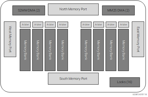
Each bank has a single read and write port. The managers that can directly access the memory are:
- The processor on this tile, which is connected to the west memory port. The processor has two 512-bit load units and one 512-bit store unit.
- The processors on 3 adjacent tiles, which are connected to the north, south and east memory ports. Each of these processors also has two 512-bit load units and one 512-bit store unit.
- The 2 S2MM and 2 MM2S DMA engines in the tile. Each DMA engine loads or stores 64-bit words.
On a given clock cycle, a memory bank can only be read by one of these managers, and written by one (the same or another) of these managers. As shown in the diagram, each bank has an arbiter module that handles attempts to access the bank by multiple managers simultaneously by stalling all the managers except one.
In this X-engine correlator I am not accessing the memories of adjacent tiles with the processors, so there are only two memory conflicts that we need to be aware of:
- The processor tries to load two 512-bit words in the same clock cycle that happen to be on the same bank. Only one word can be loaded. The next word will be stalled until the next clock cycle, delaying the execution by one clock cycle.
- The processor and a DMA engine try to load/store in the same bank in a given clock cycle. One of them will be granted access by the arbiter, and the other one will be delayed by one clock cycle.
Regarding the first conflict type, the linker is bank-aware, and it tries to put buffers into different banks to avoid this situation. However, as we will see below, when we try to use a large amount of the compute tile memory (which is advantageous to make kernel runs longer and reduce overhead as discussed above with the specific example of increasing T), it becomes more difficult to avoid cases in which the kernel wants to read at the same time from two buffers that are in the same bank. In the worst cases this can totally kill performance by completely preventing the processor from doing two 512-bit loads per clock cycle.
Luckily for us, the innermost loop of our C++ kernel only does at most one 512-bit load per clock cycle. This is a consequence of the fact that each loop iteration has 6 loads and 8 MACs, because we are operating on two elements of the array a per iteration. The naïve approach consisting of operating on one element of the array a per iteration would require 4 loads and 4 MACs, so we would have higher chances of the compiler deciding to put two loads in the same instruction because of other scheduling reasons. Therefore, in practice we do not run into this memory conflict with the inner loop of our kernel.
Regarding the second type of memory conflict, the analysis is more complex, because DMA engine transfers are somewhat non-deterministic. Most kinds of DMA transfers eventually have to flow in or out of the NPU and into the host DDR via the shimDMAs. Because access to the host DDR is shared and can have complex latency patterns, no two runs of DMA transfers are completely identical. It still helps that the linker tries to put different buffers in different banks, since typically the processor is accessing some buffers while the DMA engines are accessing different buffers (the typical case is a ping-pong buffer scheme).
I don’t think that the memory bank arbiter has any kind of priority features, which would be nice, because in workflows that are limited by compute instead of data throughput it is preferable to make the DMA engine stall instead of making the processor stall to resolve a conflict. In any case, in one run of the tracing benchmark I got a maximum kernel runtime of 2566 cycles, and the minimum is always 2553 cycles. The difference of 13 cycles is caused by memory stalls in the processor. This is only a 0.5% overhead in this worst case, which is very little. However the tracing benchmark does not run a full execution of the NPU kernel, because the trace data would be huge, so maybe there are worse cases in the full execution. In any case what really matters for performance is the average case, which is typically around 2559 cycles.
Compute tile memory usage and data flows
Once we have a C++ kernel that is able to multiply an \(8N \times 8T\) matrix \(A\) by the complex conjugate transpose of an \(8M \times 8T\) matrix \(B\), we need to decide the details of how to use it in the compute tiles. The first thing we need to keep in mind is memory usage, to make sure that whatever we need fits into the 64 KiB data memory of the compute tile. The matrix \(A\) has a size of \(128 NT\) bytes, and the matrix \(B\) has a size of \(128 MT\) bytes. The accumulator is an \(8N \times 8M\) matrix of complex int32 elements, so it has a size of \(512NM\) bytes.
Another thing to keep in mind is the data throughput of the compute tile. At the same time that the C++ kernel is working on multiplying a matrix \(A\) by another matrix \(B\) a new matrix \(A\) and a new matrix \(B\) need to be transferred into the compute tile memory by the DMA engine to be used in the next C++ kernel call. Because the DMA engines transfer 64 bits per clock cycle, it takes \(16NT\) cycles to transfer \(A\) and \(16MT\) cycles to transfer \(B\). Therefore, we are looking at a transfer duration of either \(16T \max\{N, M\}\) cycles if we transfer \(A\) and \(B\) in parallel using two DMA engines (recall that each compute tile has 2 independent S2MM DMA engines), or \(16T(N+M)\) cycles if we transfer them sequentially using a single DMA engine. On the other hand, as we have seen, the C++ kernel call requires \(4NMT\) MAC operations, so assuming a 100% efficiency (which is not real, as we have seen, but is good for initial back-of-the-envelope calculations), it will take \(4NMT\) clock cycles to run.
Therefore, in order to avoid a bottleneck caused by data transfer, we would like to make \(16T \max\{N, M\}\) be less than or equal to \(4NMT\). This gives \(N \geq 4\) and \(M \geq 4\). To put things in perspective, this means that each C++ kernel call is going to work simultaneously on the correlation of at least 32 streams against 32 other streams.
On the other hand, as mentioned above, we would like to make \(T\) as large as possible to reduce the overhead of the outer loops of the C++ kernel. However the memory size of the compute tile places a strong limit on how large we can make \(T\). Because we need to store at least two \(A\) matrices and two \(B\) matrices in the memory (the matrices on which the kernel is working currently, and the matrices which are being transferred by the DMA engines), we need \(256(N+M)T\) bytes to do that. For \(N = M = 4\), we get \(2048 T\) bytes, since the memory is only 64 KiB, this forces \(T \leq 32\), and we actually need to make it smaller than \(T = 32\), because we also need room for the accumulators.
It is clear that setting \(N = M = 4\) is advantageous compared to choosing them larger, in the sense that it allows us to make \(T\) as large as possible, thus reducing the kernel overhead. However, this means that a given compute tile will only work on a 32×32 submatrix of the output at a time. Therefore, to cover the full output, each compute tile will need to work on different 32×32 submatrices at different times, and thus use a different set of accumulators for each of these submatrices. As we are already quite constrained on compute tile memory, it is problematic to store all these sets in the compute tile memory.
My initial idea was to shuttle accumulators between the compute tile and the corresponding memory tile (which has 512 KiB of memory) on that row as needed, storing in the compute tile only two sets of accumulators (the one in progress and the one being transferred by DMA). This would force us to send \(A\) and \(B\) sequentially over the same S2MM DMA, and to use the second S2MM DMA to transfer the accumulators from the memory tile into the compute tile. This already has the disadvantage that it takes more cycles to transfer \(A\) and \(B\) sequentially, so we need to make \(N\) and \(M\) larger to avoid a data throughput bottleneck (the condition we get is \(4(N+M) \leq NM\), which is satisfied for instance for \(N = 8\), \(M = 8\)). This forces us to make \(T\) smaller (at least \(T < 16\)), and also makes the accumulators larger. Since it takes \(64 NM\) clock cycles to transfer the accumulators through the DMA engine and \(4NMT\) cycles to run the kernel, we need \(T \geq 16\) to prevent the accumulators DMA transfer from being the bottleneck, so we already see that we are going to run into some data throughput limitations.
The problem with this approach is that, as I will explain in more detail once I discuss the global data flow across the NPU array, the DMA engines are not flexible enough to allow transferring \(A\) and \(B\) sequentially over the same DMA engine if they come from different memory tiles. This kills the idea of shuttling accumulators between the compute tiles and memory tiles, and basically forces us to work with a single set of accumulators that stay fixed in the compute tile. Realizing this later on in the development (because the constraints with the DMAs only become completely clear after the global flows are designed), led me to rework major parts of the design.
Once we settle on the choice of working on a single set of accumulators in each compute tile, many other parameters get chosen naturally. The NPU on the Ryzen AI 7 350 that I’m using has 8 columns, each of which has 4 compute tiles. Therefore, it makes sense to split the correlation matrix \(K_{c,m}\) into 4×8 blocks. Each compute tile will be in charge of computing one of these blocks. The blocks should have size \(8N \times 8M\), so that each C++ kernel call amounts to correlating and accumulating a segment of \(8T\) samples from each of the streams into the block. Sequential C++ kernel calls simply accumulate sequential segments of \(8T\) samples of the same streams into the same block. Since the total size of the correlation matrix is \(32N \times 64M\) and we need \(N \geq 4\), \(M \geq 4\), it makes sense to choose \(N = 8\), \(M = 4\) to work on a 256×256 square matrix. This is where the choice of \(S = 256\) actually comes from. We can consider it as the size of the smallest square matrix in which it makes sense to make the NPU work, for otherwise we would be constrained by the data throughput of compute tiles. This also matches our initial estimates about compute and data throughput reasonably well.
Other AMD NPUs (particularly those in Versal FPGAs) have different numbers of rows and columns of compute tiles. In those NPUs it might make sense to choose slightly different values of \(N\) and \(M\) (always ensuring that \(N \geq 4\) and \(M \geq 4\), and trying to keep them not too large to allow \(T\) to be as large as possible), and we might end up having to work on a non-square correlation matrix. That is okay. It simply means that a single NPU kernel call evaluates a non-square block of the total (square) \(K_{c,m}\) correlation matrix. We can call the NPU kernel (on the same device sequentially or in multiple devices in parallel) as needed to compute all the blocks of \(K_{c,m}\) that we need, taking into account that possibly we can avoid computing some blocks due to the Hermitian symmetry. For example a 2VE38xx FPGA has 36 columns and 4 rows of compute tiles. We could set \(N = M = 4\) and make the NPU work on a 128×1152 block of the \(K_{c,m}\) matrix, which is probably excessive unless we have a massive array with thousands of antennas, or we could pretend that the 4×36 compute tiles are arranged as 12×12, and work on a 384×384 block of the \(K_{c,m}\) matrix.
Now that we have chosen \(N = 8\) and \(M = 4\), we can run the memory calculations again to choose a value for \(T\). The accumulators take 16 KiB. The linker reserves 1 KiB for the program stack. So we are left with 47 KiB for the two copies of the matrices \(A\) and \(B\), which take \(3072 T\) bytes. This gives \(T \leq 15\), so this is where the choice \(T = 15\) has come from.
The following listing is the linker script for the compute tile in row 0 and column 0. Here we can see how the linker has laid out the buffers in memory. We can ignore the variables that end in _col0_row1. These correspond to the buffers of the tile directly to the north. The hardware allows direct access to these, but we do not use this access. The base of the data memory in the address map is 0x70000, and the stack is placed right at the base and occupies 1 KiB. The accumulators (acc_to_mem_col0_row0_buff_0) are placed at offset 16 KiB (so right at the start of the second “virtual bank”) and occupy 16 KiB, so they use the whole second bank. The first copy of \(A\) begins at offset 32 KiB, at the start of the third bank. It occupies 15 KiB. The second copy of \(A\) begins at offset 48 KiB, at the start of the last bank, and also occupies 15 KiB. The first copy of \(B\) starts at offset 1 KiB, right after the stack, sharing a bank with it. It occupies 7.5 KiB. Finally, the second copy of \(B\) comes right after, at offset 8.5 KiB, occupies another 7.5 KiB, and fills the rest of this bank. Note that this allows for processor and DMA engine memory conflicts in the two copies of \(B\), since they are placed in the same bank.
MEMORY
{
   program (RX) : ORIGIN = 0, LENGTH = 0x0020000
   data (!RX) : ORIGIN = 0x7FC00, LENGTH = 0x400
}
ENTRY(__start)
SECTIONS
{
  . = 0x0;
  .text : {
     /* the __start symbol has to come at address zero. */
     *crt0.o(.text*)
     _ctors_start = .;
     _init_array_start = .;
     KEEP(SORT(*.init_array))
     _ctors_end = .;
     _init_array_end = .;
     _dtors_start = .;
     _dtors_end = .;
     *(.text*)
  } > program
  .data : {
     *(.data*)
     *(.rodata*)
  } > data
  .comment : {
     *(.comment*)
  }
  .symtab : {
     *(.symtab)
  }
  .shstrtab : {
     *(.shstrtab)
  }
  .strtab : {
     *(.strtab)
  }
  .stack_sizes : {
     *(.stack_sizes)
  }

. = 0x70000;
_sp_start_value_DM_stack = .;
. += 0x400; /* stack */
/* No tile with memory exists to the south. */
. = 0x40000;
. += 0x10000;
/* No tile with memory exists to the west. */
. = 0x50000;
. += 0x10000;
. = 0x64000;
acc_to_mem_col0_row1_buff_0 = .;
. += 0x4000;
. = 0x68000;
a_buff_0_col0_row1 = .;
. += 0x3C00;
. = 0x6C000;
a_buff_1_col0_row1 = .;
. += 0x3C00;
. = 0x60400;
b_buff_0_col0_row1 = .;
. += 0x1E00;
. = 0x62200;
b_buff_1_col0_row1 = .;
. += 0x1E00;
. = 0x6BC00;
_anonymous1 = .;
. += 0x4;
. = 0x74000;
acc_to_mem_col0_row0_buff_0 = .;
. += 0x4000;
. = 0x78000;
a_buff_0_col0_row0 = .;
. += 0x3C00;
. = 0x7C000;
a_buff_1_col0_row0 = .;
. += 0x3C00;
. = 0x70400;
b_buff_0_col0_row0 = .;
. += 0x1E00;
. = 0x72200;
b_buff_1_col0_row0 = .;
. += 0x1E00;
. = 0x7BC00;
_anonymous0 = .;
. += 0x4;
  .bss : { *(.bss*) } > data
}
INPUT(build/x_engine.mlir.prj/x_engine.o)
PROVIDE(main = core_0_2);
Global array data flows
The next step in designing the X-engine following a bottom-up approach is to design the global data flows across the NPU array. We have already decided that the array will compute a 256×256 correlation matrix, and each compute tile will work on a 64×32 submatrix of this correlation matrix. Moreover, time integration will be done in blocks of 120 samples. Therefore, the compute tile will receive a 64×120 element block \(A\) from \(A_{c,m}\) and a 32×120 element block \(B\) from \(B_{c,m}\), compute the product \(AB^*\) and add it to its accumulators. While this happens, another block \(A\) and another block \(B\) are transferred into the compute tile’s memory so they are ready for the next C++ kernel call.
The way in which these blocks \(A\) and \(B\) are distributed to the compute tiles is very similar to how the whole array matrix multiplication example in mlir-aie works. This is illustrated in the following diagram. The key idea is that each memory tile distributes a set of rows of the first matrix (the block \(A\) in our case) to a row of compute tiles and also distributes a set of columns of the second matrix (the block \(B\) in our case) to the compute tiles in its own column. In this way, each compute tile gets the inputs it needs, and the data flows without any duplications (note that each element of each matrix flows exactly once in a one-to-many flow to all the compute tiles that need to use it as an input).
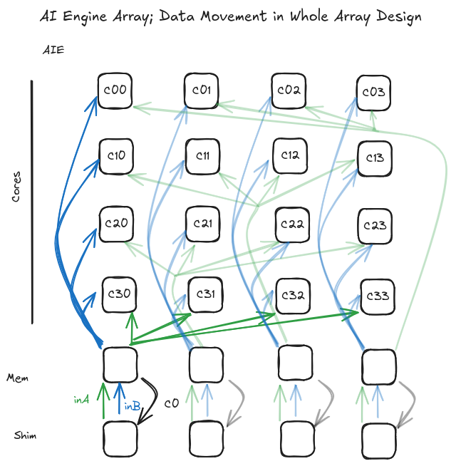
For the X-engine we adapt this idea with some minor modifications that make sense in our case. First, the Ryzen AI 7 350 NPU has 4 rows and 8 columns of compute tiles. Each column has a memory tile. Since we only need to distribute 4 blocks \(A\), as there are only 4 rows, only the memory tiles in even columns are assigned to distribute blocks \(A\). Memory tiles in odd columns are assigned to distribute blocks \(B\). Since there are 8 columns to which blocks \(B\) need to be distributed, each memory tile is in charge of two blocks \(B\), which get distributed to each of two adjacent columns simultaneously using two MM2S DMA engines in the memory tile. The point here is that blocks \(A\) have twice the size of blocks \(B\), so regarding memory usage of memory tiles it makes sense to have half of the memory tiles handle sending a block \(A\) and the other half handle sending two blocks \(B\).
To move the input data into the NPU we have 8 shimNOC tiles available, one per column. It makes sense to use one MM2S DMA engine in each tile to move data for \(A\) and another MM2S DMA engine to move data for \(B\). Now the interesting thing is the size disparity between blocks \(A\) and blocks \(B\). To account for this, we read half of the data for a block \(A\) in one shimNOC tile, and half of the data in another shimNOC tile, sending both pieces of the data to the same memory tile. In the case of blocks \(B\), since each memory tile in an odd column handles two blocks \(B\), we read each block with a different shimNOC tile and send them to the same memory tile.
Sending out the results from the compute tiles to the host DDR at the end of the correlator integration is much simpler, and it is also not performance critical because this flow has a much lower throughput than the inputs. When the integration is finished, each compute tile sends its accumulators to the memory tile on its own column. The memory tile assembles in this way a 256×32 block of the output and sends it to the shimNOC tile in the same column, which writes this block into the appropriate location in DDR.
Ethernet packet layout
Another thing we need to take into account when designing this X-engine correlator is that the input data will not be neatly laid out in DDR memory arranged in the way we want. In a complete system data will come into the correlator in Ethernet packets output by the F-engines, and the DDR memory will be arranged as a concatenation of the payloads of those packets. In many architectures there is a fully independent F-engine per antenna (or per stream), so even if multiple F-engines are implemented in the same hardware (for instance in the same FPGA), for more generality we should assume that each Ethernet packet carries data from a single stream. As part of the X-engine design, we need to design how the data is laid out in these Ethernet packets, and how the Ethernet packets get organized in DDR as they are received.
First let’s enumerate the constraints that we have for these Ethernet packets. We have already said that each Ethernet packet only carries data from one stream. The next constraint is the packet size. In order to fit into a 9000-byte Ethernet jumbo MTU without issues and leave room for packet headers, I have restricted the payload size to be 8800 bytes or less. The third constraint requires some motivation.
An F-engine typically produces sequentially (or almost sequentially) the \(C_{\mathrm{F}}\) F-engine output channels corresponding to the same time step. Some of these channels might be discarded (for instance because they lie outside of the IF bandwidth), but most of them are to be sent to different X-engines in blocks of \(C\) channels as discussed at the beginning of the post. The most natural way of sending these out is to fill up an Ethernet packet with the channel samples as they are generated, and then send it to the right host. In this approach, consecutive samples correspond to different channels. We cannot use this approach, because to use the 8×8 SIMD matrix multiplication features of the NPU we need to store contiguously in memory the real parts of 8 samples of the same channel that are consecutive in the time domain (and the same for the 8 imaginary parts). If the Ethernet packets are not laid out in this way, we will need to rearrange the data with byte-granularity, which is something that the NPU DMA engines cannot do for free with their striding support. This rearrangement will be a very expensive operation and it will completely kill the performance.
Therefore, we need to organize the Ethernet packet payloads in such a way that the data rearrangement that we need to do is not expensive (and ideally can be done with the DMA engine striding support). As we have just discussed, this forces us to place 8 real parts of samples from the same channel, and then the 8 corresponding imaginary parts. This forces us to buffer 8 time outputs of the F-engine before forming the output Ethernet packets, which requires memory. In a GPU implementation this is not a problem, but in many cases F-engines are implemented in FPGA, so we should be careful about excessive memory usage.
At this point, naïvely we would store 8 samples from different F-engine channels until we fill up the Ethernet packet. However, that also causes a performance problem. The shimNOC DMAs can stride in such a way that they read 8 samples from a given channel from one packet, then go to the next packet to read 8 samples, and so on. The problem is that the DMAs are reading from DDR, and DDR access should be done sequentially rather than striding in order to obtain good performance. Essentially, reading just 8 samples (16 bytes) and then jumping off to a different address to read another 8 samples is not a good use of DDR. I have seen experimentally that the performance is not good.
Therefore, we need to trade off between F-engine memory usage and DDR read throughput. For the sake of DDR read we would like to put as few F-engine channels and as many time-domain samples from each channel as possible into the same packet, in order to allow longer sequential DDR reads. However this forces us to increase the amount of buffering in the F-engine. Since our C++ kernel is processing data in blocks of \(8T = 120\) time-domain samples and we have already laid out the data in vectors of 8 real parts and 8 imaginary parts (8-element time-domain vectors), it makes sense to make the number of 8-element time-domain vectors per channel stored in an Ethernet packet be a multiple of \(T = 15\). I have settled on storing \(4T = 60\) 8-element time-domain vectors per channel, since otherwise performance drops measurably. On the F-engine this requires storing 480 consecutive outputs before generating an output packet. Assuming \(C_{\mathrm{F}} = 4096\), at 2 bytes per sample this requires 30 Mb of RAM (per stream). Thinking about Xilinx technology, most RFSoCs have 38 Mb of BRAM and 22.5 Mb of URAM. This means that in a typical case in which an RFSoC is handling multiple streams, external memory would be needed.
The maximum payload size of 8800 bytes together with the choice of carrying a total of 480 time-domain samples per F-engine channel implies that we can carry data from 9 F-engine channels in each packet, giving a payload size of 8640 bytes.
The data in the payload of each packet is organized as a tensor with the following dimensions:
- F-engine channel (9 channels per packet)
- Coarse time (60 coarse time blocks per packet)
- Real/imaginary part
- Fine time (8 time-domain samples per coarse time block)
These payloads are laid out in DDR in the host by making a larger tensor that adds two new dimensions to the front:
- Packet number (coarsest time dimension). A total of 136 packets per 9-channel group are processed to produce outputs \(K_{c,m}\), \(c = 1, \ldots, 9\). This number of packets is determined as the maximum that does not cause an overflow in the
int32accumulators. - Stream (256 streams to process).
An NPU kernel call processes this full DDR buffer (whose size is 286.9 MiB for each of the two inputs \(A_{c,m}\), \(B_{c,m}\), counting the total of 9 F-engine channels) to produce an output \(K_{c,m}\) for each of the 9 F-engine channels (the output size is 4.5 MiB). A larger number of F-engine channels can be handled in the same host simply by using different DDR buffers for each group of 9 channels and calling the NPU kernel for the appropriate buffers each time.
Implementation details
Implementing the design described above using mlir-aie is not completely straightforward. mlir-aie allows the developer to work at different levels of abstraction. In some cases it is possible to describe data flows using high-level object FIFOs. In other cases it is necessary to directly describe how the DMA engines are used by declaring each DMA block descriptor and each buffer manually. In most cases in this design I have had to use the latter approach.
The simplest flow is extracting the correlation results from the NPU. This flow can be realized with object FIFOs. An object FIFO sends the accumulators from each compute tile to the corresponding memory tile in the same column. To save compute tile memory, that object FIFO has only room for one object. This means that after the correlations have finished, the compute tiles must stop working until the correlation values are transferred out to the memory tiles. This is okay, because this only happens at the end of the coherent integration, so the total overhead is small. Similarly, a 1-object FIFO connects each memory tile to the corresponding shimNOC tile. The 4 object FIFOs coming from the compute tiles into the memory tile are connected to the object FIFO going from the memory tile into the shimNOC tile by using a join pattern. This means that the DMA engines will automatically concatenate the data for us.
The input flows are more complex and cannot be realized with object FIFOs. The flow of the \(A\) data works in the following way. Each shimNOC tile is configured with a task using dma_configure_task() that uses a single block descriptor to read the required data and send it out using MM2S DMA engine channel 0. This block descriptor defines a strided read in the following way (from the innermost to the outermost dimension):
- All the samples in a packet corresponding to the same F-engine channel are read (they are consecutive).
- Jump packet per packet, reading data from a packet from each stream in a group of \(4N = 32\) streams.
- Jump in the DDR buffer along the time (packet number) dimension, reading the 136 packet time steps which are needed to complete a correlator integration.
- Stride within the packet payload, jumping to each of the F-engine channels, reading the total of 9 F-engine channels carried in the packets.
This requires a 4D strided access. This has a somewhat poorly documented quirk, which is that the repeat_count of the dma_configure_task() needs to be set to the size of the outermost dimension minus one. An offset into the DDR buffer is used in each shimNOC tile so that each tile reads data from a different group of 32 streams.
The MM2S DMA engine 0 from shimNOC tiles is connected to the memory tiles manually by using the flow() call. Recall that only the memory tiles in even columns are used to store \(A\) inputs. Therefore, shimNOC tile 0 is connected to the S2MM channel 0 in memory tile 0, shimNOC tile 1 is connected to the S2MM channel 1 in memory tile 0, shimNOC tile 2 is connected to the S2MM channel 0 in memory tile 2, shimNOC tile 3 is connected to the S2MM channel 1 in memory tile 2, and so on.
The memory tiles used for \(A\) inputs have two buffers for this data, so that ping-pong buffering can be used. These buffers are organized as a tensor with the following dimensions:
- \(N = 8\) stream blocks
- \(4T\) blocks of samples
- Real/imaginary part
- 8×8 matrices of stream x time
Note that the buffer holds the data read by the two shimNOC tiles in an iteration of the two innermost dimensions of their block descriptor. Another way to understand this data is as the samples from a single F-engine channel carried in a single packet from each of \(8N\) streams (each shimNOC tile contributes \(4N\) streams).
The S2MM DMA engines of the memory tile need to receive the data from the shimNOC tile and reorganize it in memory so that it conforms to the layout given above. The S2MM channel 0 always writes to the first half of the buffer (the first 4 stream blocks), and the S2MM channel 1 always writes to the second half of the buffer. These DMAs stride in the following way, from innermost to outermost dimension:
- Write 8 consecutive samples (real or imaginary)
- Stride by 64 elements, writing all the time-domain and real/imaginary samples carried in a packet (for a single F-engine channel)
- Stride by 8 samples, writing data from 8 streams
- Jump to the appropriate places to write the data from 4 stream blocks
The MM2S DMA engine channel 0 is used to send the \(A\) input data out of the memory tile and into the corresponding row of compute tiles, which use their S2MM DMA engine channel 0 to read the data in. The flow() call is used to make these connections. The compute tile side of this flow is very simple. Each compute tile has a double buffer for \(A\) that has exactly the layout expected by a single C++ kernel call (recall that this is N x T x real/imaginary x 8 x 8). The compute tile DMA reads alternately into each of the two buffers and uses a pair of locks to synchronize with the compute tile program, implementing ping-pong buffering in the straightforward way.
The synchronization of the memory tile DMA engines is more complex and much more cumbersome to write. The memory tile needs to wait for the two inputs from the two shimNOC tiles to be fully written to the buffer, and then it can use that buffer to send 4 transfers to the compute tiles, since the memory tile holds \(4T\) blocks of samples but the compute tiles only work with \(T\) blocks at a time. This is quite tricky to do. The way I have ended up implementing it is as follows.
There are 4 locks per buffer. Let’s call them \(l_0, l_1, l_2, l_3\). Locks \(l_0\) and \(l_2\) are initialized to 1, while locks \(l_1\) and \(l_3\) are initialized to zero. The S2MM DMA engine 0 first does an AcquireGreaterEqual(1) operation on \(l_0\). This operation waits until the value of \(l_0\) is greater than or equal to 1, and atomically subtracts 1 from the lock value when it succeeds. Then it writes the data coming from the shimNOC into the first half of the buffer striding as described above. Then it does a Release(1) operation on \(l_1\). This increments the value of the lock by 1. The DMA engine now switches to the other buffer, using the corresponding locks of that buffer. It repeats these steps forever, with a chain of 2 buffer descriptors. The S2MM DMA engine 1 does the same, but using locks \(l_2\) and \(l_3\) and the second half of the buffers.
Now the tricky part is the MM2S DMA engine that is used to send the data to the compute tiles. It must wait for both \(l_1\) and \(l_3\) to be released, but the DMA engine buffer descriptor only allows performing an acquire operation on a single lock, not two. The workaround is to include a dummy buffer descriptor that does a zero-sized transfer. Therefore, the first buffer descriptor does AcquireGreaterEqual(1) on \(l_1\) and a zero-sized buffer read. The other constraint of buffer descriptors is that if a buffer descriptor acquires a lock, it must also release a lock. Therefore, this buffer descriptor does a dummy Release(0) on a lock (it doesn’t matter which lock, since Release(0) is effectively a no-op). The next buffer descriptor still needs to do AcquireGreaterEqual(1) on \(l_3\). After that, the first read of \(T\) blocks of samples can be done. This buffer descriptor must not release anything, because there are still 3 more transfers to go with the remaining \(3T\) blocks of samples. Therefore, it uses another dummy Release(0).
The next two buffer descriptors perform the next two reads of \(T\) blocks of samples. They do not use any locks. The following buffer descriptor does the final read. It will need to release a lock, but it does not need to acquire anything, so it does a dummy AcquireGreaterEqual(0) on a lock, which is also effectively a no-op. Then it transfers the last \(T\) blocks of samples and runs Release(1) on \(l_0\). We still need to release \(l_2\) as well, so there is another buffer descriptor following that has a dummy AcquireGreaterEqual(0), a dummy zero-sized read, and a Release(1) on \(l_2\). This is all it takes to transfer out the data in one of the two buffers. It is a total of 6 buffer descriptors. Then there is another set of 6 buffer descriptors that do the same with the other buffer and its set of locks. The MM2S DMA engine loops continuously through this chain of 12 buffer descriptors.
In hindsight, I could probably have used a single transfer instead of 4 to transfer all the samples out. This single transfer would be received by 4 separate transfers in the compute tile S2MM DMA engine, but I think that would work (the shimDMAs are sending data to the memory tiles in a similar way). I didn’t do this because of how the DMA engines interact with the AXI-S TLAST, which is what determines whether this approach would work, is not really documented.
Note that it is possible to do fairly complex things with the DMA engines by using an appropriate chain of buffer descriptors. However, the number of buffer descriptors is quite limited. The memory tiles have a total of 48 buffer descriptors shared among their 12 DMA channels (6 MM2S and 6 S2MM channels). The compute tiles have a total of 16 buffer descriptors shared among their 4 DMA channels (2 MM2S and 2 S2MM channels). Some ideas that I had during design simply did not work because they required too many buffer descriptors.
The memory tile MM2S DMA engine also needs to perform strided access, because it needs to read only 1/4 of the second dimension of the buffer, and the full extent of the rest of the dimensions. When designing the stride pattern for these transfers we hit another quirk, which is that the length of any dimension must be smaller than 1024. In this case, it would be most natural to read \(128 T = 1920\) elements as a single dimension, since they are consecutive in the buffer. The solution is to de-linearize this as \(T \times 128\), using the appropriate striding of \(128 \times 1\) that results in a consecutive read. This gives us the two innermost dimensions of the stride. The third and outermost dimension is simply used to read the \(N\) blocks of streams by jumping appropriately over the parts of the second dimension that are not read.
The input \(B\) is handled in a similar way. Each shimNOC DMA engine reads data using the same dimensions and striding as for \(A\). The difference is that for \(A\) the shimNOC DMAs are reading \(N/2 = 4\) blocks of streams and data from two shimNOC DMAs is joined in a memory tile to get the full \(N\) blocks of streams, while for \(B\) the shimNOC DMAs are reading \(M = 4\) blocks of streams and data from two shimNOC DMAs goes to the same memory tile but is treated fully independently because it is to be supplied to two different columns of compute tiles.
Recall that only memory tiles in odd columns are used to handle \(B\) inputs. Each of these memory tiles serves two columns of compute tiles, and it has two buffers (to implement ping-pong buffering) for each of the two columns. The dimensions of these buffers are, similarly as for the \(A\) buffers, M x 4T x real/imaginary x 8 x 8. Data comes from one shimNOC tile through the S2MM DMA engine 0 and goes to the corresponding compute tile column through the MM2S DMA engine 0. Data comes from the other shimNOC tile through the S2MM DMA engine 1 and goes to the corresponding compute tile column through the MM2S DMA engine 1. Each of these two flows work in parallel and independently in exactly the same way.
Here synchronization is more straightforward, because we don’t need to join data from two shimNOC tiles. There are just two locks per pair of (ping-pong) buffers, \(l_0\) and \(l_1\). The lock \(l_0\) is initialized to 8, and the lock \(l_1\) is initialized to zero. The S2MM engine does AcquireGreaterEqual(4) on \(l_0\), transfers the data from the shimNOC tile into the memory, writing in the appropriate strided way similarly to the \(A\) memory tiles, and does Release(4) on \(l_1\). Then it does the same with the other ping-pong buffer and repeats forever. In this way, the MM2S engine can have a series of 4 buffer descriptors, each of which has an AcquireGreaterEqual(1) on \(l_1\) and Release(1) on \(l_0\), and a transfer corresponding to the appropriate 1/4 of the buffer and using the appropriate striding similarly to what is done for \(A\). Then there are 4 more buffer descriptors for the other ping-pong buffer, and the 8 buffer descriptor chain loops forever.
Since the flows for \(A\) inputs and \(B\) inputs are kept completely separate, these data flows can operate independently and we can use the flow() call to declare statically routed flows in the NPU AXI-S interconnect. Above I mentioned that initially I tried sending \(A\) and \(B\) sequentially into the compute tiles through a single compute tile S2MM DMA engine channel. I couldn’t get this to work. Because \(A\) and \(B\) come from different memory tiles, this would require routing where multiple MM2S producers go into the same S2MM consumer, which is not allowed by static flow routing (it is limited to one-to-many). I tried to use packet routing, but still I couldn’t get a solution that would make sense and work. Another challenge I found is that I didn’t find a way to enforce that \(A\) comes before \(B\) in the compute tile S2MM DMA engine. Because these two packets are sent by different MM2S DMA engines, they could be received in any order. This means that the S2MM DMA engine would need to examine the packet header and decide based on that in which buffer to put the data, but that is not possible.
The implementation of the compute tiles is relatively simple. As mentioned above, each uses S2MM channel 0 to receive \(A\) inputs and S2MM channel 1 to receive \(B\) inputs. These are written into ping-pong buffers in the straightforward way, using just a pair of locks per channel. The program loops forever, first claiming an item (the single item) from the accumulator object FIFO for production, calling a C++ kernel that zeros out the accumulator, and then iterating according to the number of integrations done by the correlator. In each iteration, the locks for the \(A\) and \(B\) inputs are acquired, the C++ kernel that computes the matrix product is called, and the locks for the inputs are released. After all the integrations are done, the accumulator object FIFO is released, which triggers the transfer of the data to the host.
Project and code overview
The code I have written is in the x-engine directory in my mlir-aie-projects repository. The C++ kernels are implemented in x_engine.cc. The mlir-aie code is in x_engine.py. This is the most complex part of the project, mainly due to the ways in which the DMA engines need to be configured as discussed in the previous section. A run.py script is used to run the NPU kernel, either once for tracing, or repeatedly on the same inputs to obtain a preliminary benchmark. Unit testing is done with pytest and the tests in test_x_engine.py. There are simple tests such as making the inputs all zeros, all ones, and all zeros except for a single one, which are quick and effective at localizing simple mistakes (for instance indexing issues), and a complete test with random inputs that checks that the output matches the expected correlation matrix computed in Python.
There is a more complete C++ benchmark in benchmark.cc. This test runs repeatedly on pre-generated data, since it is very difficult to generate test data at the rate that the NPU kernel can process it. In fact, the test leaves the input buffers uninitialized, since their numerical values don’t really matter for the performance. Something which is quite important for this benchmark is that the buffer ownership needs to be passed from the CPU to the NPU and back according to who is going to access the buffer. This is done with a sync() method that according to what I have read in the code only handles cache coherency between the CPU and NPU. The Python API in mlir-aie automatically performs these sync() calls, so the user can mostly ignore them. The issue that I have found is that the sync() of the input data is very expensive at the rate that the NPU kernel runs. It basically takes 100% of one CPU on my Ryzen AI 7 350. I don’t know if there is a way to optimize this. I keep running again and again into cache coherency management throughput problems in several of the high-performance projects that I do, such as the Maia SDR IQ recording system (see Section V in this paper, and my FOSDEM talk).
To make the sync() overhead less bad, I have organized the C++ benchmark as two threads connected by a 4-entry ring buffer. Each entry in the ring owns an instance of the two input buffers (one buffer for \(A\) and another for \(B\)). The producer thread simply runs sync() on the buffers in the entry. The consumer thread calls the NPU kernel and syncs the results back to the host (this has much less overhead, because the output data throughput is much smaller, so it is okay to do the sync() in the same thread that is calling the NPU kernel). This threaded approach allows the sync() to run at the same time as the NPU is running the kernel, but still I get close to 100% CPU usage on the thread that is running the sync(), which isn’t great.
Benchmark results
The output of the C++ benchmark looks like this. It prints a line every 10 seconds. We can see that the throughput corresponds to around 64 Msps and the TOPS is around 33.5, which is a 57% efficiency compared to the theoretical peak TOPS of nearly 59 that this NPU can achieve. The number of NPU kernel calls per second is also important. We want to keep this low enough to avoid kernel call overhead. However, making it smaller means making the input buffers larger, and we are also limited by overflows in the 32-bit accumulators.
64.219 Msps, 33.669 TOPS, 109.306 kernel calls/s
64.063 Msps, 33.587 TOPS, 109.040 kernel calls/s
62.371 Msps, 32.700 TOPS, 106.159 kernel calls/s
64.070 Msps, 33.591 TOPS, 109.051 kernel calls/s
63.816 Msps, 33.458 TOPS, 108.620 kernel calls/s
64.159 Msps, 33.638 TOPS, 109.202 kernel calls/s
64.152 Msps, 33.634 TOPS, 109.191 kernel calls/s
64.147 Msps, 33.632 TOPS, 109.183 kernel calls/s
63.043 Msps, 33.053 TOPS, 107.304 kernel calls/s
63.564 Msps, 33.326 TOPS, 108.191 kernel calls/s
63.951 Msps, 33.528 TOPS, 108.848 kernel calls/s
64.195 Msps, 33.657 TOPS, 109.264 kernel calls/s
64.174 Msps, 33.645 TOPS, 109.228 kernel calls/s
64.258 Msps, 33.690 TOPS, 109.372 kernel calls/s
62.234 Msps, 32.628 TOPS, 105.926 kernel calls/s
63.625 Msps, 33.358 TOPS, 108.295 kernel calls/s
63.726 Msps, 33.411 TOPS, 108.466 kernel calls/s
64.354 Msps, 33.740 TOPS, 109.536 kernel calls/s
64.209 Msps, 33.664 TOPS, 109.289 kernel calls/s
64.248 Msps, 33.685 TOPS, 109.355 kernel calls/s
htop shows that one of the two threads of the benchmark is doing 100% CPU. That core is doing around 4.97 GHz. This CPU can boost up to slightly above 5 GHz, so even though htop reports 100% CPU, there is still a small margin until this thread becomes the bottleneck. The other thread, which is handling the NPU kernel launches and the sync() of the results is using basically no CPU.

Using xrt-smi examine -r all, we get the following report while the benchmark runs. One of the most interesting things is that it is reported that the NPU is using 1.1 W of power. I don’t know how accurate this reading is, but even if it is off by a large factor, it feels amazing that we can do all this compute with just 1-2 W of power. I suspect that the CPU core that is running the sync() of the inputs is using much more power, which is another reason why I don’t like this cache coherency management overhead.
System Configuration
  OS Name              : Linux
  Release              : 7.1.5-arch1-1
  Machine              : x86_64
  CPU Cores            : 16
  Memory               : 31368 MB
  Distribution         : Arch Linux
  GLIBC                : 2.44
  Model                : Laptop 13 (AMD Ryzen AI 300 Series)
  BIOS Vendor          : INSYDE Corp.
  BIOS Version         : 03.03
  Processor            : AMD Ryzen AI 7 350 w/ Radeon 860M

XRT
  Version              : 2.26.0
  Branch               : arch-staticlibs
  Hash                 : 5bc50c604f7156e35b8415c7277b236324cf9d5d
  Hash Date            : Mon, 27 Jul 2026 11:03:55 +0200
  amdxdna Version      : 2.26.0_20260727, 8ec939a647cb649acd8dc50aa5151d9302dd35eb
  virtio-pci Version   : 7.1.5-arch1-1
  NPU Firmware Version : 1.1.2.64

Device(s) Present
|BDF             |Name           |Architecture  |Topology  |
|----------------|---------------|--------------|----------|
|[0000:c2:00.1]  |NPU Krackan 1  |aie2p         |6x8       |


-------------------------------
[0000:c2:00.1] : NPU Krackan 1
-------------------------------
AIE Partitions
  Total Memory Usage: 2367 MB
  Partition Index   : 0
    Columns: [0, 1, 2, 3, 4, 5, 6, 7]
    HW Contexts:
      |PID           |Ctx ID    |Submissions  |Migrations   |Frame Evts  |Err  |Priority  |
      |Process Name  |Status    |Completions  |Suspensions  |Layer Evts  |     |GOPS      |
      |Memory Usage  |Instr BO  |             |             |            |     |FPS       |
      |              |          |             |             |            |     |Latency   |
      |--------------|----------|-------------|-------------|------------|-----|----------|
      |379409        |115       |3727         |0            |0           |0    |N/A       |
      |benchmark     |Active    |3726         |0            |0           |     |N/A       |
      |2367 MB       |120 KB    |             |             |            |     |N/A       |
      |              |          |             |             |            |     |N/A       |
      |--------------|----------|-------------|-------------|------------|-----|----------|
Platform
  Name                   : NPU Krackan 1
  Power Mode             : default
  Total Columns          : 8

Estimated Power          : 1.146 Watts
Temperature (C)          : N/A
One comment