I have a Framework Laptop 13 that has a Ryzen AI 7 350 CPU that includes an NPU. I have started playing with this NPU to understand how to develop software for it. While NPUs are mainly intended as accelerators for inference of ML models, they are fundamentally hardware accelerators for matrix multiplication and other similar linear algebra operations, so they are also useful for signal processing and other compute applications, which is why I am interested in them. Another reason why I am interested in this NPU is that, as I will explain below, it is very similar to the AIE-ML v2 AI engine in Versal FPGA SoCs, so this laptop is a great platform to learn how to use this AI engine.
NPUs use the concept of TOPS (tera operations per second) as a high-level marketing figure of their capabilities. An operation is generally understood as an addition or multiplication for int8 data types, since the amount of parallelization that can be achieved depends on the datatype width. The NPU on the Ryzen AI 7 350 is marketed as a 50 TOPS NPU. The main goal of this post is to understand where this number comes from, in terms of hardware execution units and capabilities, understand under which conditions it can be reached, and write a small application that reaches this TOPS value.
I think this is a good way of gaining in-depth understanding about a compute architecture. Most typical real world use cases are going to be slower than this, because the algorithms will have bottlenecks that result in hardware underutilization. By understanding how the hardware needs to be used to reach peak performance, we have a better idea of the gaps of these algorithms and also how to rewrite the algorithms to reduce the gap if possible. In a post last year about NEON kernels on the ARM Cortex-A53 I worked in a similar way, by choosing a simple kernel to accelerate and by comparing performance benchmarks with the peak performance allowed by the hardware.
AMD NPUs
I want to start by giving an overview of the different generations of NPUs used by AMD. They are named differently in different contexts. Knowing the equivalences between the different names can save us some time by ensuring that we are looking at the right documentation or are using the right compiler options.
AMD NPUs are fundamentally Xilinx AI Engines. The NPU on an AMD CPU and the Xilinx AI Engines on Versal FPGA SoCs are essentially identical except for the connections between the NPU/AI Engine and the rest of the system. Therefore, most of the applicable documentation and software stack, specially for low-level development, comes from Xilinx.
Xilinx currently has the following three generations of AI Engines. A comparison table can be found in the documentation:
- AI Engine. This is the oldest generation. It is present in the Versal AI Core VC1x02 series, Versal AI Edge VE1752, Versal RF series and Versal Premium VP2x02 series. According to the documentation it is optimized for DSP and communications applications.
- AIE-ML. This is the next generation, which is optimized for machine learning instead of DSP and communications. Some AI Engine features are removed, including hardware support for 32-bit floating point and integer multiplication, scalar non-linear functions such as sin/cos, sqrt and inverse sqrt, and FFT addressing modes. On the other hand, bfloat16 is added and the compute parallelism for
int8andint16is doubled. This AI engine is present in the Versal AI Core VC2x02 and Versal AI Edge VE2x02. - AIE-MLv2. It is the current generation. It is an incremental evolution of AIE-ML, and it adds new data types such as
fp8and block floating point types (MX9, MX6), and doubles the compute parallelism forint8. It is present in the Versal AI Edge Gen2 2VE3xxx series.
The architectures of these AI engine generations are called (for instance, by the C++ compilers) as follows:
- AI Engine:
aie - AIE-ML:
aie2 - AIE-MLv2:
aie2p
Beware the possible confusion here, since aie2 stands for AIE-ML, rather than AIE-MLv2.
AMD has the following generations of NPUs on their CPUs:
- XDNA. This uses the AIE-ML generation. It is present in the Ryzen 7040 CPUs (Phoenix) , and Ryzen 8040 and Ryzen 200 series CPUs (Hawk point). The array is organized in 5 columns, with 4 rows of compute tiles, for a total of 20 compute tiles. This architecture is known as
npuin some software. - XDNA2. This uses the AIE-MLv2 generation. It is present in the Ryzen AI 300 series CPUs (Strix point / Krackan point / Strix halo) and Ryzen AI 400 series CPUs (Gorgon point). The array is organized in 8 columns, with 4 rows of compute tiles, for a total of 32 compute tiles. This architecture is known as
npu2in some software.
With all this in mind, the NPU in my laptop is an XDNA2 npu2 that uses AIE-MLv2, which corresponds to the aie2p machine architecture. Therefore, in this post I will focus in this particular generation.
Update 2026-05-13: while doing more development for the Ryzen AI 7 350 NPU, I have found that the above information is not completely accurate. The XDNA2 architecture is not exactly the same as AIE-MLv2. The XDNA2 architecture is aie2p. There are some small differences with AIE-MLv2. For instance, aie2p only has 5 accumulator registers, as indicated by the llvm-aie sources. aie2p is definitely the same as XDNA2, because the llvm-aie PR that added support for it explicitly mentioned Strix, and the xrt-smi tool on my laptop reports that architecture. There is a second architecture called aie2ps, which was also called Telluride in its corresponding llvm-aie PR. This architecture has 8 accumulator registers, which matches the documentation in the AIE-MLv2 architecture manual. Additionally, it seems that Telluride is AMD’s codename for the first Versal Gen 2 chips. This is all quite badly documented and somewhat confusing, specially because the low level documentation for Xilinx’s AIE engines is much better than the documentation for AMD NPUs (for instance there is no equivalent of the AIE-MLv2 architecture manual for XDNA2). It looks like the differences between aie2p and aie2ps are minor (so far I have spotted this difference in the number of accumulators, and also differences in block-floating point support and related registers). So in what follows I will still treat AIE-MLv2 and XDNA2/aie2p interchangeably, since their differences do not matter for this post.
AIE-MLv2 architecture
Xilinx AI engines, as well as AMD NPUs, are organized as arrays of tiles. The following figure shows an example AIE-MLv2 array.
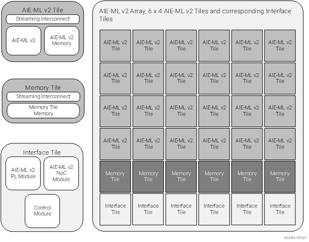
The bottom row of the array, which is row zero, is composed by interface tiles that provide connectivity to the rest of the system. These tiles are substantially different in the Xilinx AIE-MLv2 engines and in the AMD XDNA2 NPUs, since in the AIE-MLv2 engines they provide connectivity to the FPGA and the SoC interconnect, while in the XDNA2 NPUs they provide connectivity to the CPU complex.
The next one or two rows (counting from the bottom) are memory tiles, each of which contains 512 KiB of memory. This is sometimes referred to as L2 memory, but I do not like this term, because this is not cache memory that is transparent to the programmer. All the data movement in memory is explicitly controlled by the programmer.
The remaining rows are compute tiles, also known simply as “tiles” or core tiles. Each of these tiles contains one processor, which I will describe below in more detail, 64 KiB of data memory (sometimes called L1 memory), and 16 KiB of program memory. Each of these processors is fully independent and runs code from its own program memory. This means that each compute tile can be programmed to execute a different algorithm, or an algorithm can be distributed in parallel over multiple compute tiles.
In AMD XDNA2 NPUs, the array always has 8 columns, one row of memory tiles, and 4 rows of compute tiles, for a total of 32 compute tiles and 8 memory tiles. In Versal AI Edge Series Gen 2, the array size depends on the part size (see the datasheet). 2VE33xx have 12 columns with one memory tile and 2 compute tiles, for a total of 24 compute tiles and 12 memory tiles. 2VE35xx have 24 columns with one memory tile and 4 compute tiles, for a total of 96 compute tiles and 24 memory tiles. 2VE38xx have 36 columns with two memory tiles and 4 compute tiles, for a total of 144 compute tiles and 72 memory tiles.
Tiles in the AIE-MLv2 are interconnected in three different ways, which are depicted in the diagram shown below. First, there are AXI4-Stream buses that run across the whole engine in horizontal and vertical directions and which meet on an AXI4-Stream interconnect at each tile’s location. This forms an engine-wide AXI4-Stream interconnect system that is able to move data from any tile to any other tile. Data movement between the local memory on the tile and the AXI4-Stream interconnect is mainly done by DMA engines on the tile. From the point of view of the programmer, this is the most flexible and easiest to use data movement mechanism.
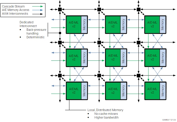
Second, each tile can access directly the local memory of neighbouring tiles. The way this is drawn with blue lines is potentially misleading, because it appears that each tile can access data from each of its four adjacent tiles. However, the documentation says: “The architecture is designed to enable each AIE-ML v2 unit to interface with up to four distinct memory modules. These modules encompass: The module placed towards the west, Its own local memory module, The module positioned to the north, The module situated to the south”. Note that the diagram actually intends to represent this accurately. On the horizontal direction there are bidirectional blue arrows connecting each green AIE-ML v2 tile to the memory module of the tile to the west, but there is no arrow connecting to the memory module of the tile to the east. On the other hand, on the vertical direction there are two bidirectional blue arrows connecting both the green tile to the memory module of the tile to the south, and to the memory module of the tile to the north.
Third, there is a cascade connection that allows a tile to send a 512-bit accumulator value to a tile immediately to the right or down. These two data movement mechanisms are more advanced and I will not use them in this post.
In the case of XDNA2 NPUs, the interface tiles at the bottom of the array are known as shimNOC tiles. They contain shimDMAs that perform data movement between the main memory of the CPU complex (passing through the L3 cache) and the NPU array, by moving data through the AXI4-Stream interconnect.
AIE-MLv2 processor
Each AIE-MLv2 compute tile contains a processor that is a 32-bit RISC in-order exposed-pipeline VLIW SIMD vector processor. Let us unpack what all of this means. First, VLIW (very long instruction word) means that the architecture uses long instructions (up to 128 bits per instruction), each of which can contain an instruction for each of the functional units of the processor, which are:
- Two load units (A and B), each with its own address generation unit (AGU)
- One store unit, with its own AGU
- A scalar unit with an integer ALU
- A register move unit, that can copy the value from one register to another
- A vector SIMD unit that can perform integer and floating point arithmetic
Since each VLIW instruction can contain an independent instruction for each functional unit, it is easier to make the functional units work simultaneously and avoid bottlenecks.
Exposed-pipeline means that the processor does not pretend to the programmer that each instruction executes in order as an atomic unit. We know that a CPU pipeline requires a certain number of cycles until the result of an instruction is available (whether it is a load from memory, a calculation, or even a jump). A traditional CPU hides this latency to the programmer by pretending that the results of an instruction are available to the subsequent instructions, and stalling or reordering instructions if the results are not available yet when an instruction needs them. In contrast, an in-order exposed-pipeline architecture makes the pipeline visible to the programmer. This kind of processor always executes one instruction per cycle in order and generally does not stall (except when the processor is waiting on a hardware lock, for instance to synchronize with a DMA, or another similar situation). The results of an instruction are only visible to instructions that happen a given number of clock cycles afterwards.
This is best illustrated by the following example from the llvm-aie fork used for these processors. In this example, loads have a latency of 8 cycles, and scalar multiplications have a latency of 3 clock cycles.
1: lda r12, [p0]     // writes r12 after cycle 8.
2: nop
3: nop
4: mul r12, r12, r12 // reads r12 initial value and writes r12
                     // after cycle 6.
5: mov r14, r12      // reads r12 initial value
6: nop
7: add r13, r12, r6  // reads r12 from instruction 4.
8: nop
9: mul r14, r12, r7  // reads r12 from instruction 1.
An exposed-pipeline architecture requires the compiler to know exactly how the timing of each instruction works. This allows the compiler to schedule instructions optimally for this particular processor and gives deterministic performance. It is quite hard to write assembly by hand for an exposed-pipeline processor, since any mistakes with instruction timing mean that we might be looking at the wrong data, rather than stalling the processor. On the other hand, it is much easier to read assembly and understand the timing and find performance losses, since we know that the processor always runs at one instruction per cycle and any nops inserted by the compiler mean that it is not able to schedule optimally. Something else to keep in mind is that this approach only works well if the timing of all the instructions is deterministic. This is possible for the AI engine processors because generally they only access their local memory, so memory accesses do not need to go through caches that introduce non-determinism. There is still the possibility of contention in more advanced cases, for example when processors access the memory of neighbouring tiles. In these cases the processor simply stalls until the contention is resolved.
Finally, SIMD vector processor means that the processor is mainly intended to be used as a vector processor using SIMD instructions. This is something that we are already familiar with from AVX and NEON SIMD instructions in x86-64 and ARM CPUs. The AIE-MLv2 processor has a scalar unit, but the processor is not very fast (around 1.8 GHz in AMD NPUs, and 1 GHz for Versal), so the way to get any significant amount of compute done is through the vector execution unit. The scalar unit is only intended as support, so the mindset for writing code for these AI engines is very similar to the mindset for writing SIMD-heavy code in x86-64 or ARM.
However, there is a fundamental difference between the AIE-MLv2 SIMD vector unit and SIMD in x86-64 and ARM CPUs. In AVX and NEON we are used to doing mostly pointwise operations on SIMD vectors. For instance, a 512-bit vector contains 64 int8 elements, and we can operate on two of these vectors by performing their pointwise sum or multiplication, thus performing 64 operations in parallel. If we can perform a pointwise multiply-accumulate, then we can get 128 operations in parallel by performing the multiplications and additions in the same instruction. In AIE-MLv2 we can still do this, but the architecture is heavily focused on matrix multiplication, so it contains SIMD instructions to perform multiplication of small matrices stored in vector registers. These instructions are the only way of fully leveraging all the hardware compute resources and getting anywhere close to peak TOPS.
As an example, which will become relevant when we analyse how the SIMD characteristics of AIE-MLv2 are related to the TOPS of the Ryzen AI 7 350 NPU, let us say that instead of treating 512-bit vectors as vectors of 64 int8 elements, we treat them as 8×8 matrices of int8 elements. The multiplication of two of these small matrices requires 512 multiplications, because each entry in the resulting 8×8 matrix requires 8 multiplications as we multiply a row of the first matrix by a column of the second matrix. These 8 multiplications also need to be added together, which requires 7 additions, or 8 if we think about adding the resulting matrix to an existing accumulator instead of just producing the result. Therefore, a multiply-accumulate of two 8×8 matrices requires 512 multiplications and 512 additions, for a total of 1024 operations. There is no way in which we can get so many operations by doing pointwise operations on vectors, unless the vector size was unrealistically large.
Therefore, the SIMD instructions for matrix multiplication provide a way to perform a massive number of hardware multiply-accumulate operations by combining the entries of SIMD vectors of reasonable size in multiple ways (8 possible products involving each entry, as opposed to just one product per entry for pointwise operations). A multiplication of larger matrices can be efficiently decomposed into these SIMD operations that perform multiply-accumulate of small matrices. Other similar operations from linear algebra can be optimized in the same way.
The AIE-MLv2 processor has 12 512-bit SIMD vector registers called x0, x1, ..., x11. These registers can be grouped in pairs to form 1024-bit registers called y0, y1, ..., y5. However, most SIMD instructions operate on 512-bit values. Additionally, there are 8 2048-bit accumulator registers (update: aie2p has only 5 accumulator registers). These registers are used in the multiply-accumulate instructions, both to store the output and to serve as an additional input. They are so wide to allow for bit growth in the accumulations. They can be used either as 64-element 32-bit vectors, which is the configuration used for accumulation of 64-element 8-bit operands and other small integer types, or as 32-element 64-bit vectors, which is the configuration used for accumulation of larger integer operands, or as 64-element float32, which is the configuration used for all floating point operands.
Theoretical peak TOPS
The way to make best use of the hardware and achieve peak TOPS is by using the SIMD vector processor to perform multiply-accumulate of small matrices. The size of these matrices, and hence the number of MACs (multiply-accumulate scalar operations) per SIMD instruction depends on the data type. The following table summarizes some of the supported data types, listing the maximum number of MACs in a matrix multiply-accumulate operation for those data types, explaining how the accumulator is laid out for this operation (SPFP stands for single-precision floating point, which is just float32). This table is expanded in the intrinsics user guide, which contains additional combinations of data types and lists the matrix sizes that achieve these MACs.
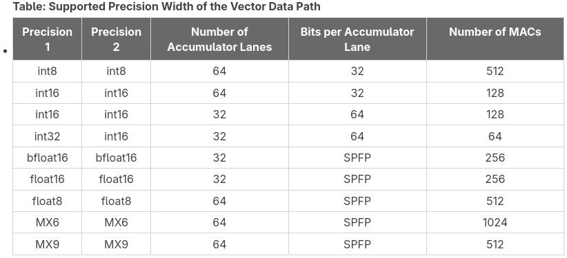
Since we are interested in comparing with the published value of 50 TOPS, we will be using int8 operands, as presumably that value corresponds to this case. The intrinsics user guide shows that int8 types can be operated as matrix multiplication of 8×8 times 8×8. This is the example I just gave above, which achieves 512 MACs. Another supported configuration is to perform a 4×8 times 8×16 matrix multiplication. Note that this also has 512 MACs, and it requires a 1024-bit vector as the second operand. I will be working with the 8×8 times 8×8 matrix multiplication, since it is easier to use, due to the symmetry in the operands.
Since each MAC is counted as two operations (a multiplication and an addition), the theoretical TOPS can be calculated as
TOPS = 2 * MACs * compute tiles * clock frequency (Hz) * 1e-12
For the int8 8×8 times 8×8 matrix multiplication we have 512 MACs, and the Ryzen AI 7 350 NPU has 32 compute tiles. I haven’t seen any source that clearly states the clock frequency at which the NPU runs, but this can be benchmarked easily, and we will do it below. It is 1.8 GHz, and it seems that the clock frequency is fixed. This calculation gives us 58.9824 TOPS. Therefore, it makes sense that AMD publishes a value of 50 TOPS for this NPU, as they are probably factoring in an overhead typical of a more realistic use case, and also giving a round number that looks nicer for marketing. The higher-end Ryzen AI 9 375 and HX 470 are marketed as 55 TOPS, and the Ryzen AI 9 HX 475 is marketed as 60 TOPS. I suspect that the difference is just due to these NPUs running at a slightly higher clock frequency, since the array structure is supposed to be the same for all the XDNA2 NPUs.
Note that the table above lists 1024 MACs for MX6 block floating point operands. This is achieved by 4×16 times 16×16 matrix multiplication. These MX6 values use 4 bits per value in a 512-bit SIMD register. These 4 bits correspond to the magnitude, since the signs, shifts and exponents are stored in dedicated registers F, G, E. Therefore, a 512-bit vector can store 128 MX6 values. A 16×16 matrix needs a 1024-bit vector. By using MX6 operands in this configuration, we could achieve 117.9648 TOPS. However, in this post I will be using int8 operands to validate the 50 TOPS marketing figure.
Development environment
There are different frameworks for developing code to run on AMD NPUs. The main software repository is RyzenAI-SW, but this is heavily geared to running popular ML frameworks, such as ONNX, on the NPU. There is another framework called mlir-aie that provides a lower level approach, which is aligned better with my interests, so this is what I will be using in this post.
mlir-aie contains a Python framework called IRON that generates LLVM MLIR code representing a workload that runs on the NPU, including the code that runs on each compute tile processor and the configuration of DMAs and other hardware. Kernels for the compute tile processor can be written in C++ and compiled either with the open-source llvm-aie Peano compiler, which is a fork of LLVM that adds support for the Xilinx AI engine processors, or with the closed-source Xilinx CHESS compiler, which is included in Vitis. In simple cases the kernels can also be directly written in Python with IRON.
The LLVM MLIR code, together with any object code compiled from C++ by Peano or xchess, is processed by the aiecc compiler, which runs LLVM passes through the MLIR code and generates an xclbin image and a file with binary instructions for the NPU. These two files are what the runtime needs to load on the NPU to run the workload. Loading and running these files on the NPU can be done either in Python or in C++.
Something that I like a lot about mlir-aie is that it has good documentation, including a programming guide with exercises, and lots of examples. The best order in which to go through this information is not too clear from the README. I have done the following:
- Go through the mini tutorial, which quickly gives an overview of how IRON looks like and what are the hardware capabilities of the NPU from the point of view of the programmer.
- Go through the programming guide, which reintroduces everything from the mini tutorial in more detail, introduces the “placed” syntax for IRON, and includes additional topics. Sections 5 and 6 in the guide are basically pointers to the examples, so I have only selected the examples I was mainly interested in.
- There is also a set of MLIR exercises that I haven’t covered yet. These are about writing MLIR by hand, which can be useful in more advanced use cases and also to fully understand the MLIR output generated by IRON.
IRON has two different levels of abstraction, which are introduced in section 1 of the programming guide. In the highest level of abstraction, the programmer declares objects and optionally has the ability to constrain in which tiles they are placed. Otherwise, the compiler will try to place the objects automatically. The lower level of abstraction is known as “placed”, since objects need to be explicitly constructed in a given tile. The two levels of abstraction are not so different, since the objects that are constructed are essentially the same, although some operations are done differently. The syntax is also different, so I find this slightly confusing, as there are essentially two parallel syntaxes in IRON that cannot be mixed together. In this post I will be using the highest level of abstraction, but I will be manually placing the objects.
Additionally, IRON supports JIT compilation. This allows defining an NPU workload in the same way, but it handles the MLIR generation, compilation and loading automatically when the JIT kernel is called.
To install all the software stack in my laptop, where I’m running Arch Linux, I have first gone to the xdna-driver repository and used the instructions to build packages for Arch. Later I found that this does not install libxilinxopencl.a, which is required by some mlir-aie examples. Therefore, I had to go back and rebuild XRT (which is a submodule of xdna-driver) by adding -cmake "-DXRT_STATIC_BUILD=ON" to the build.sh call and by doing some small changes to the repository.
Once xdna-driver is installed, we can run xrt-smi validate to test that the NPU and software stack are working correctly.
$ xrt-smi validate
WARNING: User doesn't have admin permissions to set performance mode. Running validate in default mode
Validate Device           : [0000:c2:00.1]
    Platform              : NPU Krackan 1
    Power Mode            : default
-------------------------------------------------------------------------------
Test 1 [0000:c2:00.1]     : gemm
    Details               : TOPS: 51.0
    Test Status           : [PASSED]
-------------------------------------------------------------------------------
Test 2 [0000:c2:00.1]     : latency
    Details               : Average latency: 72.0 us
    Test Status           : [PASSED]
-------------------------------------------------------------------------------
Test 3 [0000:c2:00.1]     : throughput
    Details               : Average throughput: 70697.0 op/s
    Test Status           : [PASSED]
-------------------------------------------------------------------------------
Validation completed
There is also an xrt-plugin-amdxdna package in the official Arch repository, but I couldn’t get this to work properly, since xrt-smi validate complained that it was missing the xclbin files for the tests.
After installing xdna-driver, I have installed mlir-aie by following the instructions. Something to keep in mind about mlir-aie’s examples is that they have been tested mostly in Windows, so some things, particularly examples that have host C++ code, don’t work out of the box. The changes needed to get these working are simple:
- Most
CMakeLists.txtfiles are missing aproject()statement, and it needs to be added belowcmake_minimum_required(). - Some
CMakeLists.txtinsist on setting the C compiler to gcc-13. This can be removed, since the C compiler is autodetected correctly.
The best example to test that mlir-aie is working is the first exercise in the mini-tutorial. This is a Python script that uses JIT to build the NPU code.
Implementation of peak-tops application
Here we finally reach the main goal of this post, which is to walk through the implementation of a simple example that achieves a TOPS close the theoretical peak value, understanding how the example works and where are the places where performance is lost.
C++ kernel
The project I have implemented can be found here. First I will explain the C++ kernel that is run in the compute tile processors. The code is as follows.
void peak_tops(
    v64int8 *__restrict a, v64int8 *__restrict b0,
    v64int8 *__restrict b1, v64int8 *__restrict out) {
  event0();

  constexpr int N = 16384;
  constexpr int num_vectors = N / 64;

  v64acc32 acc0 = {};
  v64acc32 acc1 = {};

  for (int i = 0; i < num_vectors; ++i) {
    v64int8 x = *a++;
    acc0 = mac_8x8_8x8(x, *b0++, acc0);
    acc1 = mac_8x8_8x8(x, *b1++, acc1);
  }
  out[0] = ssrs(acc0, 0);
  out[1] = ssrs(acc1, 0);

  event1();
}
This kernel takes in three buffers a, b0, b1 containing 16384 int8 elements each. It interprets each buffer as 256 8×8 matrices (in row-major order). It also takes an output buffer out that has room for 128 int8 elements, interpreted as two 8×8 matrices. The kernel computes the 256 matrix multiplications of each matrix in a and each matrix in b0 and adds them together, writing the result to out[0]. Likewise, the kernel computes the 256 matrix multiplications of each matrix in a and each matrix in b1, writing the result to out[1]. I will explain later why we are dealing with b0 and b1 instead of just a single buffer b.
Note that the operation performed by this kernel is an ingredient for the multiplication of larger matrices. For example, if we wanted to multiply two 2048×2048 matrices A and B, we could call this kernel 32768 times to compute an 8×16 block of the output in each call, by passing to the kernel a block of 8 rows of A into the buffer a and two adjacent blocks of 8 columns of B into the buffers b0 and b1. The elements in the buffers would need to be arranged in the order which is expected by this kernel, but this can be achieved by the DMA engines on the tiles, which support multi-dimensional addressing schemes that can be used to reshape the data as it is transferred. The point I want to make is that this example kernel is not just a silly example intended to make the NPU work hard, but it is a basic building block for matrix multiplication, which is what the NPU is designed to do most efficiently.
Let us go through the kernel in detail. It heavily uses C intrinsics for the AI-MLv2 architecture, which are documented in the AI Engine-ML v2 Intrinsics User Guide. Other generations of Xilinx AI engines have similar intrinsics and user guides. There is also a higher-level C++ API that provides portability across different generations by allowing higher-level constructs and compiling down to the best intrinsics on each architecture. I will not be using this C++ API here, since I prefer to work with low-level intrinsics.
The v64int8 datatype is a vector of 64 int8 elements, and it is defined in the intrinsics API. The v64acc32 datatype denotes a vector of 64 int32 elements used in an accumulator register. These accumulators are set to zero by initializing them with the empty constructor.
I have found that Peano can be quite finicky about the way that the C++ code is written, with equivalent constructs yielding quite different assembly. For instance, when using a[i] to address buffer elements, the compiler would generate instructions to perform loads by using the AGU to compute the address in terms of an offset in the dj0 register. On the other hand, using *a++ results in using a post-increment in the load instructions, which is a much better approach.
We use the mac_8x8_8x8() intrinsic to perform the 8×8 times 8×8 matrix multiplication and accumulate the results in one of the two accumulators. All the supported multiply-accumulate intrinsics for int8 operands are described here.
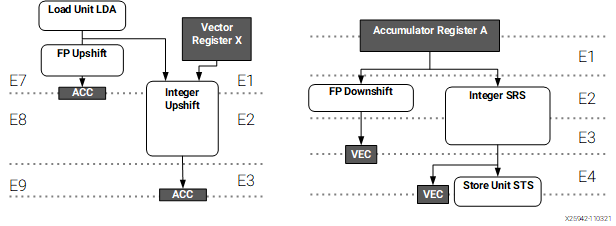
The figure below shows how the integer datapath for the vector execution unit of the AIE-MLv2 is organized. We see that the pipeline has 6 stages, so it takes 6 clock cycles between the issuing of the instruction and the moment when the accumulator is updated. On the other hand, the accumulator value is read in stage 4. This means that it only takes 2 clock cycles to update the accumulator.
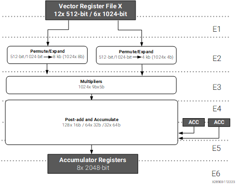
Integer path for the vector execution unit, taken from the AIE-MLv2 architecture manual
The consequence is that we cannot keep using the same accumulator in every clock cycle, as we need to wait two clock cycles for the result to be updated before using the accumulator again. This is quite typical with accumulate instructions in any kind of processor architecture, since adding to the same accumulator represents a long data dependence chain. The way around this limitation is to use multiple accumulators. For instance, in this case, if we alternate between two accumulators, we can execute a multiply-accumulate instruction per clock cycle. This is the reason why we are multiplying one buffer a with two buffers b0 and b1. If the use case we have in mind is the multiplication of a large matrix, these are operations we need to do anyway, so no work is wasted. If we only had to compute the products for one buffer a and one buffer b, we could still do it by alternating between two accumulators and adding both at the end. However, I didn’t find a way for the compiler to do this properly, even though I think that I wasn’t getting into architectural limitations, as I will explain in more detail below with the assembly code.
Once we have finished our multiply-accumulate operations, we need to put the results of the accumulators back into memory. Since the accumulator is wider that the operand data types, in order to account for bit growth, we need to narrow down the result before storing it to memory. There is a dedicated shift-round-saturate (SRS) path that goes from the accumulator registers to the store unit, shown in the rightmost path of the figure below. This is how accumulator values get stored to memory. The intrinsic to do this SRS for 32-bit to 8-bit integer conversion is ssrs(). The second argument of this intrinsic is the shift that needs to be applied. Typically this would be a scale factor that compensates bit growth. Here we do not have any particular fixed point representation in mind for our int8 values, so I am arbitrarily using zero as shift. However this will cause saturation for most input values, since we are adding 256 products of two int8‘s.
The event0() and event1() intrinsics generate dedicated event instructions in the processor that are used for tracing. I will explain this in more detail later. It is quite common to add these instructions at the beginning and end of each kernel to measure how long it takes to execute.
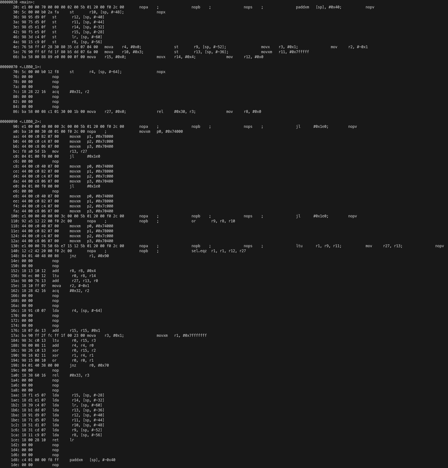
We can compile the project and show the assembly for the full ELF file that will run on each compute tile processor by running just show-asm. Here I show only the code corresponding to the peak_tops() function.
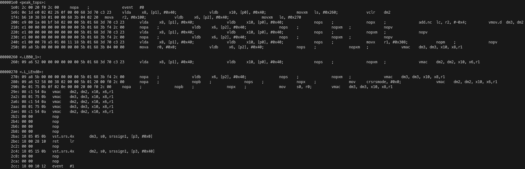
The kernel receives its pointer arguments a, b, c and out in the pointer registers p0, p1, p2, p3 respectively. The processor has 8 20-bit registers that are used for pointers. Since the processor only has a 1 MiB address map, it does not need 32-bit pointers. After the event #0 instruction, which generates an EVENT_0 trace event signalling the kernel start, the load units A and B are used simultaneously to load v64int8 vectors from b0 and a into SIMD registers x8 and x10 respectively. A post-increment of 64 bytes is used on the pointer registers in these instructions. This is the most straightforward to manage memory accesses, since we are accessing memory linearly in this kernel.
The same VLIW instruction also moves the constant 0x260 to the loop start register ls and uses the vector unit to clear the accumulator dm2. Here we see the power of the VLIW architecture in action, as just the first instruction of the kernel has performed two 512-bit loads in parallel and done other setup needed by utilizing four execution units of the processor.
The loop start register ls is used in combination with the loop end register le and loop count register lc for hardware control of the innermost loop without using jump instructions. These registers work as follows: after the instruction on the address indicated by le is executed, if lc is non-zero, it is decremented and the execution jumps to the address indicated by ls instead of continuing with the next instruction.
The next VLIW instruction is moving the value 256 into the general-purpose 32-bit register r2 (the processor has 32 of these registers) using the load unit A. Note that, besides performing memory loads, load units can alternatively be used to load a register with a value that is either a constant or calculated with simple integer arithmetic supported by the AGU. In this case, this is done because the same instruction also uses the move unit to move the value 0x270 into the loop end register. Additionally, this instruction loads a v64int8 from p2 into x6, performing a 64-byte post-increment of the pointer.
Memory loads have a latency of 7 cycles, so the next few instructions are going to pipeline more of these loads following the same pattern before the multiply-accumulate operations can begin. In addition to these loads, some of these VLIW instructions contain other things that are needed to set up the execution. An add of r2 and the constant -4 is used to set the loop counter to 252. This makes sense, because the C++ loop has 256 iterations, but in the assembly 4 of these iterations are unrolled out of the loop because of instruction scheduling reasons. The vector unit is used to move dm2 to dm3, therefore also initializing the accumulator dm3 to zero. The constant 0x308 is moved to r1. As we will see momentarily, the ISA has a single vmac instruction to perform any kind of SIMD multiply-accumulate operation. The configuration of this operation (which in this case is 8×8 times 8×8 matrix multiplication of int8 operands) is encoded in a general-purpose register that is used as operand in the instruction. Finally, the value zero is moved to r0. This is what will be used to set the SRS shift below.
7 clock cycles after the first loads the first vmac instruction runs. We see that it is quite straightforward. It uses two x SIMD registers, an accumulator register, and a configuration general-purpose register as input operands, and an accumulator register as destination.
The next two instructions are the kernel loop. The kernel alternatively loads values from p0 and p1 while performing the vmac of the values that were loaded from p0 and p2 8 and 7 cycles ago respectively, and then loads a value from p2 while performing the vmac of the values that were loaded from p0 and p1 7 cycles ago.
Since in this second instruction we are only using one of the load units, it seems quite possible to load another value from another pointer and use this value instead of the value loaded from p0 in the other instruction. However, I have not found a way for Peano to generate this kind of code without adding many other seemingly unnecessary instructions that kill the throughput. That is the reason why this kernel is using a and b0, b1, instead of using just a and b by interleaving two accumulators.
After the loop finishes, we have one final load and 7 vmac operations to finish the pipeline. In addition to this, the constant zero is moved to the crsrsmode register. This control register is not well documented, although it appears in the intrinsics user guide as a 1-bit register that controls the mode of SRS operations. The register r0, which had been loaded with zero previously, is moved to the s0 register, which is a special 6-bit register that controls the SRS shift (there are 4 of these registers).
Due to the latency of 6 cycles of the vmac instructions, the first result store needs to come 6 cycles after the vmac that uses the corresponding accumulator. For this reason, 4 nop cycles need to be inserted. The store performs an SRS operation using the shift in register s0, and writes to the memory indicated by the pointer p3.
After this store we have the function call return instruction, which uses the link register for the jump. The latency of this jump is also taken into account, because after it we have the second result store and the event #1 instruction.
The exposed-pipeline architecture makes it very easy to count how many cycles a piece of code takes to run. The main loop of this kernel has two instructions, does one vmac per instruction and runs 252 times. Outside of the loop we have 27 instructions and 8 vmac instructions among them. Therefore, the kernel does a total of 512 vmac operations, as expected from the C++ code, and takes 531 cycles to run. The efficiency, in terms of vmac per clock cycle is 96.4%, which is reasonably good.
IRON code and MLIR
A Python script uses the IRON API do generate MLIR code that defines how the NPU is configured and how the C++ kernel is called. I’m using the high-level syntax of IRON, but I’m specifying the placement of the objects manually.
For the sake of simplicity, I’m calling the C++ kernel with buffers that are allocated in the local memory of each compute tile, and not doing any data movement between the CPU complex and the NPU. A realistic use case would need to move some data from main memory into the NPU, and then retrieve the results, but doing such data movement in a way that it does not become the bottleneck can be a whole subject on its own depending on the amount of data that needs to be transferred.
The kernel needs input buffers a, b0, and b1. I am allocating each of these as a buffer of 16384 int8 elements, which is what the kernel expects. The reason for using this size is that the local memory for the compute tiles is 64 KiB, and it also needs to have some room for the program stack, so 16384 bytes is the largest power of two size for which we can allocate three buffers in local memory. In addition, the kernel needs an output buffer, but that only has 128 int8 elements. All these buffers are allocated in the local memory of each compute tile.
The same program is run in each of the 32 compute tiles. The rest of the IRON code is mainly dedicated to synchronization. We want to start all the kernels at the same time (or close enough) and wait for all of them to finish before terminating the execution of the NPU workload. Since the main way to achieve synchronization within the IRON framework is by doing data movement with object FIFOs, I’m sending a dummy uint32 value as some sort of synchronization token. I have chosen a 32-bit datatype because this matches the word size of the AXI-S interconnect, which has 64-bit buses supporting two words in parallel.
Starting all the kernels synchronously is easy, because object FIFOs can be used with a broadcast pattern, as they can have one producer and many consumers. In this way, a single object FIFO is used to synchronize the start of all the kernels. The runtime sequence, which is what controls the high-level execution of the NPU, produces a token on the object FIFO at the start of the execution, each compute tile has a consumer for this object FIFO, and the compute tile program waits to consume an object on the FIFO before calling the C++ kernel.
Waiting for all the kernels to finish is trickier. The object FIFOs support a join pattern in which an object FIFO consumes an object from each of multiple object FIFOs, concatenates these objects and produces the concatenated object as a result. The offsets used for the concatenation are specified manually, and they can all be set to zero, which results in the multiple objects overwriting each other without increasing the resulting object size. This is ideal for dummy uint32 values used as synchronization tokens.
Ideally, we would like to do the opposite of what we do for the start: use a join pattern to consume a synchronization token from each of the 32 compute tiles, join all the tokens, and produce a single token on which the runtime sequence can wait. The issue with this is that there are not enough DMAs to do it. Implemented naïvely, this approach would require 32 S2MM (stream to memory map) DMAs on the shimNOC tile that is used for the join, since each of the join consumers needs to use its own S2MM DMA to fetch data from the AXI-S interconnect into the memory of the tile. However, shimNOC tiles only have 6 S2MM DMAs. We can try to implement a hierarchical approach with a tree of joins. For instance we can do a 4-element join on each memory tile to join all the compute tiles of the corresponding column (each memory tile also has 6 S2MM DMAs). But then we still have an issue because we would need to join the 8 columns in a shimNOC tile, which still goes above the DMA limit. I tried to add another layer to join columns in pairs before finally joining the 4 pairs in a shimNOC tile, but I was getting errors during MLIR generation. I’m not fully sure if the hardware really can support this, and if so, whether the IRON object FIFOs can support this pattern (the DMAs can also be configured manually for advanced use cases not supported by object FIFOs).
In the end, what I have done is to join each of the columns, and then do a loop in the runtime sequence where I consume a token from each column. This is not ideal, because I would have liked this synchronization to happen using the hardware in the array, rather than because of iteration in the runtime sequence, but for the purposes of this peak-tops demo, it is fine.
The MLIR code can be generated by running just mlir. It is placed in build/peak_tops.mlir. Here I will comment some portions of the code, which allow us to understand better how the NPU is set up.
First, variables are declared for each of the NPU tiles. Since I have done explicit placing in IRON, each tile is already assigned to concrete coordinates in the array. Otherwise the coordinates would show up as (?, ?) and would be determined when the MLIR is compiled. Note that compute tiles are called CoreTile in MLIR.
%logical_core = aie.logical_tile<CoreTile>(0, 2)
%logical_core_0 = aie.logical_tile<CoreTile>(0, 3)
[...]
%logical_core_29 = aie.logical_tile<CoreTile>(7, 4)
%logical_core_30 = aie.logical_tile<CoreTile>(7, 5)
[...]
%logical_shim_noc = aie.logical_tile<ShimNOCTile>(0, 0)
%logical_mem = aie.logical_tile<MemTile>(0, 1)
%logical_mem_31 = aie.logical_tile<MemTile>(1, 1)
%logical_shim_noc_32 = aie.logical_tile<ShimNOCTile>(1, 0)
[...]
%logical_mem_43 = aie.logical_tile<MemTile>(7, 1)
%logical_shim_noc_44 = aie.logical_tile<ShimNOCTile>(7, 0)
The object FIFO used to synchronize the start of the kernels is declared as an object FIFO that has the shimNOC at coordinates (0, 0) as producer and each of the 32 compute tiles as consumer. The FIFO consists of one 32-bit value, since I have set all these synchronization FIFOs to a depth of one object (the default is two objects).
aie.objectfifo @start_fifo(%logical_shim_noc,
  {%logical_core, %logical_core_0, %logical_core_1,
  %logical_core_2, %logical_core_3, %logical_core_4,
  %logical_core_5, %logical_core_6, %logical_core_7,
  %logical_core_8, %logical_core_9, %logical_core_10,
  %logical_core_11, %logical_core_12, %logical_core_13,
  %logical_core_14, %logical_core_15, %logical_core_16,
  %logical_core_17, %logical_core_18, %logical_core_19,
  %logical_core_20, %logical_core_21, %logical_core_22,
  %logical_core_23, %logical_core_24, %logical_core_25,
  %logical_core_26, %logical_core_27, %logical_core_28,
  %logical_core_29, %logical_core_30}, 1 : i32)
 : !aie.objectfifo>
The object FIFOs used for the termination synchronization of each column are declared as follows (here I show only the FIFOs for the first column). An object FIFO has the memory tile on that column as producer and the shimNOC tile on that column as consumer. For each compute tile in the column there is another object FIFO with that tile as the producer and the memory tile as the consumer. The join of these four object FIFOs is implemented as an object FIFO link in which the four FIFOs are joined together using offsets of zero.
aie.objectfifo @termination_fifo_col0(%logical_mem,
  {%logical_shim_noc}, 1 : i32)
 : !aie.objectfifo<memref<1xui32>>
aie.objectfifo @termination_fifo_col0_core00(%logical_core,
  {%logical_mem}, 1 : i32)
 : !aie.objectfifo<memref<1xui32>>
aie.objectfifo @termination_fifo_col0_core01(%logical_core_0,
  {%logical_mem}, 1 : i32)
 : !aie.objectfifo<memref<1xui32>>
aie.objectfifo @termination_fifo_col0_core02(%logical_core_1,
  {%logical_mem}, 1 : i32)
 : !aie.objectfifo<memref<1xui32>>
aie.objectfifo @termination_fifo_col0_core03(%logical_core_2,
  {%logical_mem}, 1 : i32)
 : !aie.objectfifo<memref<1xui32>>
aie.objectfifo.link [@termination_fifo_col0_core00,
 @termination_fifo_col0_core01, @termination_fifo_col0_core02,
 @termination_fifo_col0_core03] ->
 [@termination_fifo_col0]([0, 0, 0, 0] [])
The buffers are declared for each compute tile as follows.
%a_buff_core00 = aie.buffer(%logical_core) {
  sym_name = "a_buff_core00"} : memref<16384xi8>
%b0_buff_core00 = aie.buffer(%logical_core) {
  sym_name = "b0_buff_core00"} : memref<16384xi8>
%b1_buff_core00 = aie.buffer(%logical_core) {
  sym_name = "b1_buff_core00"} : memref<16384xi8>
%out_buff_core00 = aie.buffer(%logical_core) {
  sym_name = "out_buff_core00"} : memref<128xi8>
The C++ kernel is declared as an external function.
func.func private @peak_tops(memref<16384xi8>,
  memref<16384xi8>, memref<16384xi8>, memref<128xi8>)
 attributes {link_with = "build/peak_tops.o"}
Then a program for each compute tile is declared. The program in IRON is as follows. It first consumes an object from the start FIFO, then calls the C++ kernel for a large number of iterations, and then produces an object in the termination FIFO.
def core_fn(start, termination, a, b0, b1, out, kernel):
    start.acquire(1)
    start.release(1)
    for _ in range_(iterations):
        kernel(a, b0, b1, out)
    termination.acquire(1)
    termination.release(1)
The MLIR equivalent is here. We see that it is pretty much line-to-line equivalent. There are variables for a subview access into the objects in the FIFOs after the object is acquired, but these variables are never used, so they will be optimized out. Something else we note is that the whole program is wrapped in an “almost while true” which is realized as for loop with 2**63 iterations. This is because by default in IRON the compute tile function run as a while true unless otherwise specified.
%core_0_2 = aie.core(%logical_core) {
  %c0 = arith.constant 0 : index
  %c9223372036854775807 = arith.constant 9223372036854775807
                          : index
  %c1 = arith.constant 1 : index
  scf.for %arg0 = %c0 to %c9223372036854775807 step %c1 {
    %0 = aie.objectfifo.acquire @start_fifo(Consume, 1)
         : !aie.objectfifosubview<memref<1xui32>>
    %1 = aie.objectfifo.subview.access %0[0]
         : !aie.objectfifosubview<memref<1xui32>> ->
           memref<1xui32>
    aie.objectfifo.release @start_fifo(Consume, 1)
    %c0_45 = arith.constant 0 : index
    %c8388608 = arith.constant 8388608 : index
    %c1_46 = arith.constant 1 : index
    scf.for %arg1 = %c0_45 to %c8388608 step %c1_46 {
      func.call @peak_tops(
        %a_buff_core00, %b0_buff_core00, %b1_buff_core00,
        %out_buff_core00)
        : (memref<16384xi8>, memref<16384xi8>,
           memref<16384xi8>, memref<128xi8>) -> ()
    }
    %2 = aie.objectfifo.acquire @termination_fifo_col0_core00(
         Produce, 1) : !aie.objectfifosubview<memref<1xui32>>
    %3 = aie.objectfifo.subview.access %2[0]
         : !aie.objectfifosubview<memref<1xui32>> ->
           memref<1xui32>
    aie.objectfifo.release @termination_fifo_col0_core00(
      Produce, 1)
  }
  aie.end
}
Finally, we have the runtime sequence, which specifies how the host system interacts with the NPU to execute the workload, mainly through the use of shimDMAs in shimNOC tiles.
The shimNOC DMA used for the start FIFO is configured with a buffer descriptor (dma_bd) that transfers a single i32 element. Note that these DMAs, as well as the DMAs in the other tiles, support 4D memory access with striding, in order to perform advanced data access patterns as part of data movement, which is extremely useful for many matrix and tensor operations. Each shimNOC DMA for a termination FIFO is also configured in the same way. An issue_token is enabled, since we will be waiting for the completion of that DMA. Finally, the sequence waits for each of the 8 termination DMAs and frees the task of the start FIFO DMA.
aie.runtime_sequence(%arg0: memref<1xui32>,
 %arg1: memref<1xui32>) {
  %0 = aiex.dma_configure_task_for @start_fifo {
    aie.dma_bd(
      %arg0 : memref<1xui32>, 0, 1,
      [<size = 1, stride = 0>, <size = 1, stride = 0>,
       <size = 1, stride = 0>, <size = 1, stride = 1>])
      {burst_length = 0 : i32}
    aie.end
  }
  aiex.dma_start_task(%0)
  %1 = aiex.dma_configure_task_for @termination_fifo_col0 {
    aie.dma_bd(
      %arg1 : memref<1xui32>, 0, 1,
      [<size = 1, stride = 0>, <size = 1, stride = 0>,
       <size = 1, stride = 0>, <size = 1, stride = 1>])
      {burst_length = 0 : i32}
    aie.end
  } {issue_token = true}
  aiex.dma_start_task(%1)
  [...]
  aiex.dma_await_task(%1)
  aiex.dma_await_task(%2)
  aiex.dma_await_task(%3)
  aiex.dma_await_task(%4)
  aiex.dma_await_task(%5)
  aiex.dma_await_task(%6)
  aiex.dma_await_task(%7)
  aiex.dma_await_task(%8)
  aiex.dma_free_task(%0)
}
This MLIR code has some higher-level constructs that are replaced by lower-level objects during compilation. We can look at the results of this translation by running just xclbin to compile the project and looking at build/peak_tops.mlir.prj/input_with_addresses.mlir, which is intended to support tracing.
Object FIFOs are replaced with producers and consumers that are implemented with buffers and hardware locks. For instance, this is the producer for the termination FIFO on a compute tile.
%termination_fifo_col7_core31_buff_0 = aie.buffer(%tile_7_5) {
  address = 1152 : i32, mem_bank = 0 : i32,
  sym_name = "termination_fifo_col7_core31_buff_0"}
 : memref<1xui32>
%termination_fifo_col7_core31_prod_lock_0 = aie.lock(
  %tile_7_5, 2) {init = 1 : i32,
  sym_name = "termination_fifo_col7_core31_prod_lock_0"}
%termination_fifo_col7_core31_cons_lock_0 = aie.lock(
  %tile_7_5, 3) {init = 0 : i32,
  sym_name = "termination_fifo_col7_core31_cons_lock_0"}
Flows in the AXI-S interconnect are declared. This interconnect generally uses static circuit switching, which is set up by these flows, but it can use packet switching, which routes dynamically depending on packet IDs. This shows the flows from the shimNOC tile to all the compute tiles used for the start FIFO, and the flows from the compute tiles on each column to four S2MM DMAs in the memory tile in that column and the flow from such memory tile to the shimNOC tile in that column, which is how the termination FIFOs are implemented.
aie.flow(%shim_noc_tile_0_0, DMA : 0, %tile_7_5, DMA : 0)
aie.flow(%shim_noc_tile_0_0, DMA : 0, %tile_7_4, DMA : 0)
[...]
aie.flow(%shim_noc_tile_0_0, DMA : 0, %tile_0_2, DMA : 0)
aie.flow(%mem_tile_0_1, DMA : 0, %shim_noc_tile_0_0, DMA : 0)
aie.flow(%tile_0_2, DMA : 0, %mem_tile_0_1, DMA : 0)
aie.flow(%tile_0_3, DMA : 0, %mem_tile_0_1, DMA : 1)
aie.flow(%tile_0_4, DMA : 0, %mem_tile_0_1, DMA : 2)
aie.flow(%tile_0_5, DMA : 0, %mem_tile_0_1, DMA : 3)
[...]
Since object FIFOs have been replaced with hardware locks, the program for the compute tiles also uses these locks instead of object FIFO operations. For instance, this is how an object from the start FIFO is consumed.
aie.use_lock(%start_fifo_0_cons_cons_lock_0,
             AcquireGreaterEqual, 1)
aie.use_lock(%start_fifo_0_cons_prod_lock_0, Release, 1)
DMAs, including their buffer descriptors, in compute and memory tiles are also set up. This is how the DMAs in a compute tile are configured. An S2MM DMA is used to consume from the start FIFO. It has a single buffer descriptor that uses the hardware lock to claim access to the buffer, then performs the memory transfer, releases the buffer, and jumps again to the same buffer descriptor. The producer for the termination FIFO that sends a token to the memory tile is an MM2S DMA that is set similarly.
%mem_0_2 = aie.mem(%tile_0_2) {
  %0 = aie.dma_start(S2MM, 0, ^bb1, ^bb2)
^bb1:  // 2 preds: ^bb0, ^bb1
  aie.use_lock(%start_fifo_0_cons_prod_lock_0,
               AcquireGreaterEqual, 1)
  aie.dma_bd(%start_fifo_0_cons_buff_0 : memref<1xui32>, 0, 1)
   {bd_id = 0 : i32, next_bd_id = 0 : i32}
  aie.use_lock(%start_fifo_0_cons_cons_lock_0, Release, 1)
  aie.next_bd ^bb1
^bb2:  // pred: ^bb0
  %1 = aie.dma_start(MM2S, 0, ^bb3, ^bb4)
^bb3:  // 2 preds: ^bb2, ^bb3
  aie.use_lock(%termination_fifo_col0_core00_cons_lock_0,
               AcquireGreaterEqual, 1)
  aie.dma_bd(%termination_fifo_col0_core00_buff_0
   : memref<1xui32>, 0, 1) {
      bd_id = 1 : i32, next_bd_id = 1 : i32}
  aie.use_lock(%termination_fifo_col0_core00_prod_lock_0,
               Release, 1)
  aie.next_bd ^bb3
^bb4:  // pred: ^bb2
  aie.end
}
Memory tiles have a much more complex DMA setup, since they need to perform the join operation. An MM2S DMA is used to send the data to the shimDMA. Because of the join operation, the send is distributed over 4 buffer descriptors, each of which uses the buffer and lock corresponding to the object FIFO where data arrives from the compute tile. Note that because we have used an offset of zero for all the join elements instead of using different offsets to concatenate the data, all the buffer descriptors except the last one result in a size of zero. So effectively what this DMA is doing is to consume an object from the first 3 FIFOs without sending anything, and then sending an object from the fourth FIFO.
%memtile_dma_1_1 = aie.memtile_dma(%mem_tile_1_1) {
  %0 = aie.dma_start(MM2S, 0, ^bb1, ^bb5)
^bb1:  // 2 preds: ^bb0, ^bb4
  aie.use_lock(%termination_fifo_col1_cons_lock_0,
               AcquireGreaterEqual, 1)
  aie.dma_bd(%termination_fifo_col1_buff_0 : memref<1xui32>,
             0, 0) {bd_id = 0 : i32, next_bd_id = 1 : i32}
  aie.use_lock(%termination_fifo_col1_prod_lock_0, Release, 1)
  aie.next_bd ^bb2
^bb2:  // pred: ^bb1
  aie.use_lock(%termination_fifo_col1_cons_lock_1,
               AcquireGreaterEqual, 1)
  aie.dma_bd(%termination_fifo_col1_buff_0 : memref<1xui32>,
             0, 0) {bd_id = 1 : i32, next_bd_id = 2 : i32}
  aie.use_lock(%termination_fifo_col1_prod_lock_1, Release, 1)
  aie.next_bd ^bb3
^bb3:  // pred: ^bb2
  aie.use_lock(%termination_fifo_col1_cons_lock_2,
               AcquireGreaterEqual, 1)
  aie.dma_bd(%termination_fifo_col1_buff_0 : memref<1xui32>,
             0, 0) {bd_id = 2 : i32, next_bd_id = 3 : i32}
  aie.use_lock(%termination_fifo_col1_prod_lock_2, Release, 1)
  aie.next_bd ^bb4
^bb4:  // pred: ^bb3
  aie.use_lock(%termination_fifo_col1_cons_lock_3,
               AcquireGreaterEqual, 1)
  aie.dma_bd(%termination_fifo_col1_buff_0 : memref<1xui32>,
             0, 1) {bd_id = 3 : i32, next_bd_id = 0 : i32}
  aie.use_lock(%termination_fifo_col1_prod_lock_3, Release, 1)
  aie.next_bd ^bb1
^bb5:  // pred: ^bb0
Four S2MM DMAs are used to receive the data from each of the compute tiles in the row. Each DMA has a single buffer descriptor that performs a transfer by using locks for synchronization. The first 3 DMAs have a transfer size of zero, so the DMA just drops the incoming AXI-S packet instead of writing it to memory, but it still uses the hardware locks to register that a packet has arrived. The fourth DMA has a transfer size of 1, so it is the one that actually passes the dummy value to the join operation.
  %1 = aie.dma_start(S2MM, 0, ^bb6, ^bb7)
^bb6:  // 2 preds: ^bb5, ^bb6
  aie.use_lock(%termination_fifo_col1_prod_lock_0,
               AcquireGreaterEqual, 1)
  aie.dma_bd(%termination_fifo_col1_buff_0 : memref<1xui32>,
             0, 0) {bd_id = 4 : i32, next_bd_id = 4 : i32}
  aie.use_lock(%termination_fifo_col1_cons_lock_0, Release, 1)
  aie.next_bd ^bb6
^bb7:  // pred: ^bb5
  %2 = aie.dma_start(S2MM, 1, ^bb8, ^bb9)
^bb8:  // 2 preds: ^bb7, ^bb8
  aie.use_lock(%termination_fifo_col1_prod_lock_1,
               AcquireGreaterEqual, 1)
  aie.dma_bd(%termination_fifo_col1_buff_0 : memref<1xui32>,
             0, 0) {bd_id = 24 : i32, next_bd_id = 24 : i32}
  aie.use_lock(%termination_fifo_col1_cons_lock_1, Release, 1)
  aie.next_bd ^bb8
^bb9:  // pred: ^bb7
  %3 = aie.dma_start(S2MM, 2, ^bb10, ^bb11)
^bb10:  // 2 preds: ^bb9, ^bb10
  aie.use_lock(%termination_fifo_col1_prod_lock_2,
               AcquireGreaterEqual, 1)
  aie.dma_bd(%termination_fifo_col1_buff_0 : memref<1xui32>,
             0, 0) {bd_id = 5 : i32, next_bd_id = 5 : i32}
  aie.use_lock(%termination_fifo_col1_cons_lock_2, Release, 1)
  aie.next_bd ^bb10
^bb11:  // pred: ^bb9
  %4 = aie.dma_start(S2MM, 3, ^bb12, ^bb13)
^bb12:  // 2 preds: ^bb11, ^bb12
  aie.use_lock(%termination_fifo_col1_prod_lock_3,
               AcquireGreaterEqual, 1)
  aie.dma_bd(%termination_fifo_col1_buff_0 : memref<1xui32>,
             0, 1) {bd_id = 25 : i32, next_bd_id = 25 : i32}
  aie.use_lock(%termination_fifo_col1_cons_lock_3, Release, 1)
  aie.next_bd ^bb12
^bb13:  // pred: ^bb11
  aie.end
}
Compute tile program
Above I have shown the assembly for the C++ kernel that is run in the compute tiles. Here I will show the rest of the program’s assembly, so that we can understand exactly what gets run.
The processor begins running on the __start symbol at address 0x0 in program memory. This routine just jumps to a __main_init function that is placed at the end of the program and initializes the stack pointer to 0x70000. This is because the local memory of the compute tile is mapped at 0x70000-0x80000. The stack is placed at the beginning of local memory and grows upwards. The local memory of adjacent compute tiles is mapped at other offsets in the address map: west 0x50000-0x60000, north 0x60000-0x70000, south 0x40000-0x50000 (I haven’t found documentation for this, so I’ve reverse-engineered it from the linker scripts for this peak-tops example, as they also show the symbols for adjacent tiles). Recall that the local memory of the tile to the east is not directly accessible, so it is not part of the memory map.
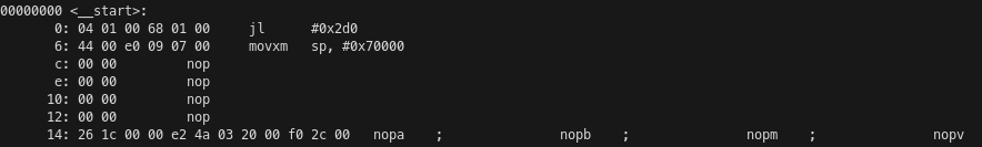
The _main_init function has the typical structure of a non-leaf function that follows the ABI. The first instruction is a jump and link to the main function at address 0x20, but since jumps have a latency of 5 cycles, the following 5 instructions are also executed before jumping. The stack pointer is incremented to make room for saving the registers lr and p7. I don’t know what p7 is being used for in this function, since it is set to the old stack pointer value but is never read. The registers p0 and r1 are set to zero. I believe they are respectively the char** argv and int argc arguments of a typical C main() function. After the main function returns, execution continues at address 0x300, which has a done instruction. This instruction somehow indicates the hardware that the program has finished its execution, but I don’t know exactly what it does. The saved registers are restored from the stack, the stack frame is popped, and the function returns to its caller.
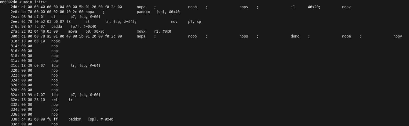
The main() function is quite long but it is not complicated. It begins with a preamble that saves a bunch of registers to the stack. Then the acq and rel instructions are used to acquire and release the start FIFO locks. The loop that calls the C++ kernel many times starts at address 0x90 and has been partially unrolled by four iterations. We have a jump and link instruction that performs the function call, and after it (but executing before the jump) are the moves that set the arguments of the kernel, which are the four pointers to buffers in local memory. Then there is some logic to determine when to keep iterating on this loop, and another pair of acq and rel instructions that acquire and release the termination lock. Because IRON defaults to running a while true loop, there is a loop that is endless in practice. It begins at address 0x70 and there is some logic before address 0x198 that determines if the jump should be taken. After this jump there is code which never executes in practice due to the loop. This code restores the saved registers and stack and returns to the caller.
We had calculated that the C++ kernel takes 531 cycles to run. Due to the way that the main() function calls the kernel, there are 6 extra cycles to perform each call, plus an additional 8 cycles (3 instructions until the jump, including it, plus 5 cycles of latency following the jump) for every 4 calls due to the loop logic. Therefore, the average number of cycles per C++ kernel run is 539. This leads to an efficiency of 95%.
Runtime code
To run our code on the NPU, we need to declare buffers in the host to be used as inputs and outputs of the NPU workload. These are the buffers used by the runtime sequence that we wrote in IRON to transfer data between the host and the NPU using shimDMAs. We need to load the xclbin file that contains the kernel and the NPU instructions file that contains control code that runs on a microcontroller in the NPU. Then we can execute the kernel on the NPU. All this can be done either in Python by using IRON or in C++ by using the XRT API. For this project I have used IRON for simplicity. I have a simple Python script that runs the kernel and performs some benchmark calculations. This script can optionally enable tracing, which is described next.
Tracing
The compute tiles can use tracing to report events as packets on the AXI-S interconnect. These packets are routed to a shimDMA that copies them to a buffer in memory. The buffer can be analysed after the workload has executed. This is a great way to profile the NPU execution. In order to enable tracing, I’m doing a slightly different configuration, because it does not seem possible to have tracing enabled plus all the 32 compute tiles and their object FIFOs. I am only using 2 compute tiles per column, with tracing enabled in all of them, and I am only calling the C++ kernel 1024 times, since otherwise the trace would be massive.
Tracing can be run with just trace. This prints the following trace summary, which counts the number of kernel invocations and the cycles that each invocation took by using the events generated by the event0 and event1 instructions in the kernel. The number of cycles is being counted as 530 instead of 531 probably because one of these event instructions is not being counted in the calculation of their timestamp differences. It seems that some events are being lost on one of the tiles, which leads to wrong results for the cycle count.
core_trace for tile2,0
Total number of full kernel invocations is 1024
First/Min/Avg/Max cycles is 530/ 530/ 530.0/ 530
core_trace for tile3,0
Total number of full kernel invocations is 1024
First/Min/Avg/Max cycles is 530/ 530/ 530.0/ 530
core_trace for tile2,1
Total number of full kernel invocations is 1011
First/Min/Avg/Max cycles is 530/ 422/ 530.7339268051434/ 940
core_trace for tile3,1
Total number of full kernel invocations is 1024
First/Min/Avg/Max cycles is 530/ 530/ 530.0/ 530
core_trace for tile2,2
Total number of full kernel invocations is 1024
First/Min/Avg/Max cycles is 530/ 530/ 530.0/ 530
core_trace for tile3,2
Total number of full kernel invocations is 1024
First/Min/Avg/Max cycles is 530/ 530/ 530.0/ 530
core_trace for tile2,3
Total number of full kernel invocations is 1024
First/Min/Avg/Max cycles is 530/ 530/ 530.0/ 530
core_trace for tile3,3
Total number of full kernel invocations is 1024
First/Min/Avg/Max cycles is 530/ 530/ 530.0/ 530
core_trace for tile2,4
Total number of full kernel invocations is 1024
First/Min/Avg/Max cycles is 530/ 530/ 530.0/ 530
core_trace for tile3,4
Total number of full kernel invocations is 1024
First/Min/Avg/Max cycles is 530/ 530/ 530.0/ 530
core_trace for tile2,5
Total number of full kernel invocations is 1024
First/Min/Avg/Max cycles is 530/ 530/ 530.0/ 530
core_trace for tile3,5
Total number of full kernel invocations is 1024
First/Min/Avg/Max cycles is 530/ 530/ 530.0/ 530
core_trace for tile2,6
Total number of full kernel invocations is 1024
First/Min/Avg/Max cycles is 530/ 530/ 530.0/ 530
core_trace for tile3,6
Total number of full kernel invocations is 1024
First/Min/Avg/Max cycles is 530/ 530/ 530.0/ 530
core_trace for tile2,7
Total number of full kernel invocations is 1024
First/Min/Avg/Max cycles is 530/ 530/ 530.0/ 530
core_trace for tile3,7
Total number of full kernel invocations is 1024
First/Min/Avg/Max cycles is 530/ 530/ 530.0/ 530
Tracing also generates a JSON file that can be opened with Perfetto. Because of how Perfetto works, each clock cycle is represented as one microsecond. We need to be mindful of this, since the clock cycle of 1.8 GHz actually gives 0.555 ns per cycle.
In Perfetto, we see that at the beginning of the trace each compute tile spends a while in LOCK_STALL. This is because the program is waiting to acquire the lock used for the start object FIFO. Then there is another LOCK_STALL event that corresponds to releasing the lock (it only lasts one clock cycle), an INSTR_EVENT_0 that corresponds to the first instruction of the C++ kernel, and the start of execution of vector instructions some cycles afterwards. Note that the compute tiles start at slightly different times. Probably this is due to different latencies of the AXI-S interconnect that distributes the start packet to all the tiles.
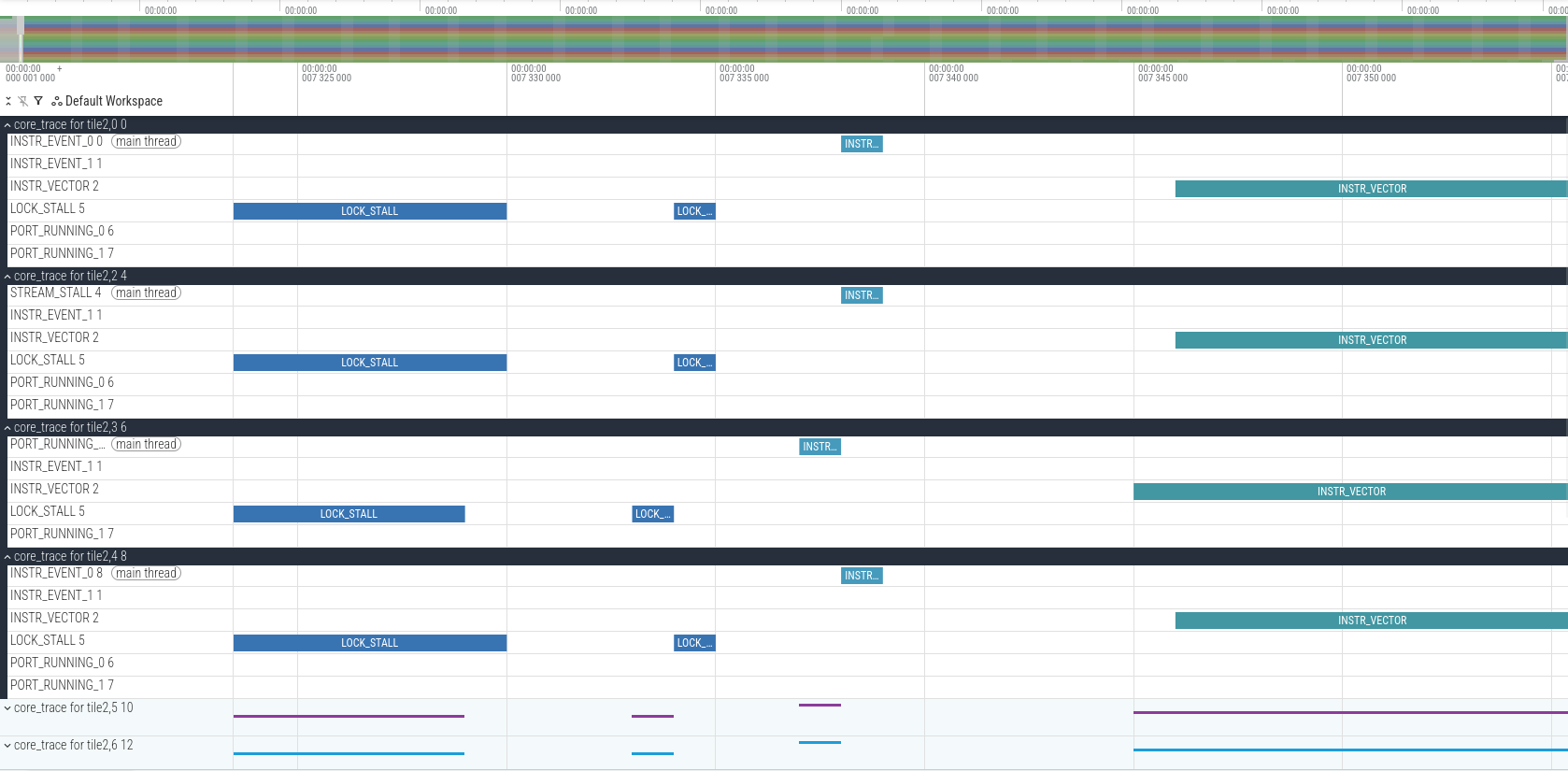
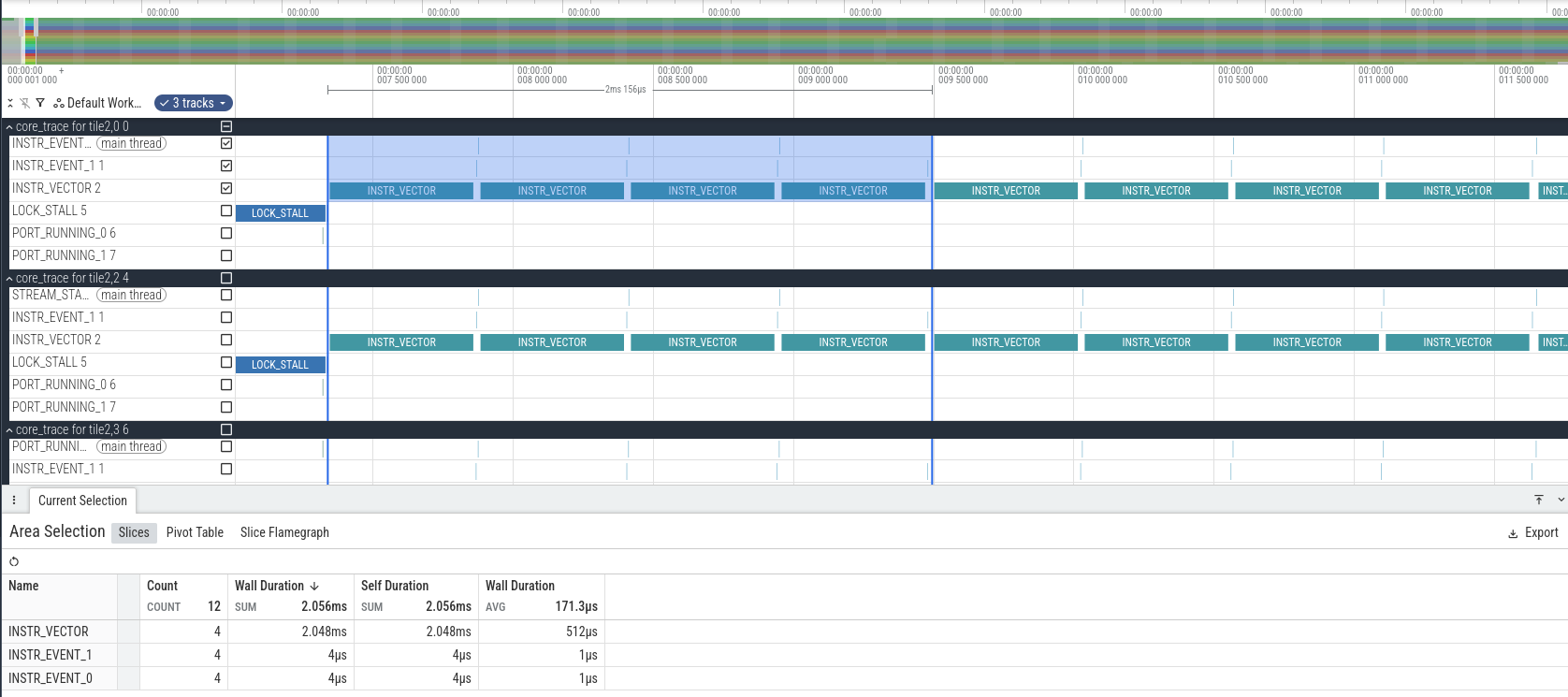
We can also calculate how many clock cycles it takes to run 4 executions of the C++ kernel. The result is 2156 clock cycles, which corresponds to 539 cycles per call, which matches what we had computed by analysing the assembly.
Running the benchmark
The benchmark of the peak-tops kernel can be run with just run. This builds the kernel with a large number of iterations (2**23) so that it takes a couple seconds to run. Note that by default NPU kernel executions time out if they take more than a few seconds.
The IRON API measures for us how much time the kernel execution took. We can use this value to perform two calculations. First, since we know that the kernel takes 539 clock cycles per iteration, we can estimate the clock frequency used by the compute tile processors. I get a value of 1.808 GHz, so it seems that the nominal clock frequency of the NPU on the Ryzen AI 7 350 is 1.8 GHz. It does not seem to use frequency scaling of any sort.
Second, we can compute the TOPS. We know that each call to the C++ kernel computes 512 matrix products of two 8×8 matrices. Each of these matrix products requires 512 MACs. Therefore, each C++ kernel call does 262144 MACs, which is 524288 operations. Multiplying this by the number of iterations and by the number of compute tiles (32), and dividing by the execution time, which is 2.501 seconds, we get 56.28 TOPS. This is in line with what we expected. The theoretical peak TOPS at 1.8 GHz is 58.9824, and we have determined that our kernel has an efficiency of 95%. Therefore, we would expect to get 56.03 TOPS. It makes sense that we measure a slightly higher value because the clock frequency we have measured is slightly higher than 1.8 GHz.
Code
All the code used in this post can be found in my mlir-aie-projects/peak-tops repository.
That’s really interesting, I’ve been reading about NPUs too. It seems like a whole new area for software development.