In February this year I was in the Spanish amateur microwave radio conference Micromeet 2025. In this conference, Luis Cupido CT1DMK presented a simple and inexpensive 10 GHz transverter that he called Nes-Transverter, with the motto “Instant microwaves. Just add solder”. The main idea of this design is that it is very simple and can be built by anyone with just a handful of inexpensive components. Luis was hoping that this project would help more people get on the 10 GHz band in a hands-on way, and he also wanted to demystify some ideas such as amateur microwave radio being difficult or expensive.
The schematic for this design is available here. It uses a 144 MHz IF, allowing it to be connected to a VHF amateur radio. An ADF4351 synthesizer, to be sourced from an inexpensive AliExpress dev board, generates a 2.556 GHz LO with complementary outputs. These two outputs are used in a frequency doubler built with two BAT15 diodes to produce a 5.112 GHz LO, which is filtered with a transmission line stub and amplified with an MMIC such as the ERA 3+. A harmonic x2 mixer built with two BAT15 diodes directly connected to the waveguide probe uses the 5.112 GHZ LO and the 144 MHz IF to produce 10.368 GHz, which is the usual frequency for terrestrial narrowband communications in the 10 GHz amateur band.
I was very interested by this talk, and thought that it would be fun to play with this project, since I haven’t done any hands-on electronics projects in quite a while. However, rather that building a transverter for narrowband communications, I decided to adapt the ideas to build a 10 GHz FMCW radar. I wanted to build a cheaper version of the ADALM-PHASER, minus the phased array part. The Phaser is an educational development kit from ADI that demonstrates concepts in phased array beamforming and FMCW radar. It uses an ADF4159 waveform generator synthesizer and a HMC735 VCO as a 12.2-12.7 GHz LO source that can be programmed to generate FMCW waveforms such as a linear sawtooth and triangle chirps. An ADALM-PLUTO or another SDR is used as a 2.2 GHz IF to obtain 10-10.5 GHz via high-side LO injection. On the transmit section, the 10-10.5 GHz signal is sent to an SMA connector to drive an external antenna. On the receive section, a 4×8 phased array of patches is included in the PCB. Each column of 4 patches is phased as a single element by connecting them together on the PCB. The 8 columns are beamformed in groups of 4 with two ADAR1000, which allows choosing independent complex coefficients for each column. Each of the 4-column beamformer outputs is connected to an RX channel of a 2-channel SDR, so that the final beamforming step can happen in software (see here for a block diagram of the Phaser).
The first thing I needed to replace in Luis design to convert it to an FMCW radar was the LO source. Since I will be using an SDR rather than a VHF radio as the IF, I could use an LO of around 4-4.5 GHz, which would give me around 10-10.5 GHz with an IF around 1-2 GHz. This meant that I could use the ADF4158 synthesizer as the LO source. This is the cheaper variant of the ADF4159, and it only goes up to 6.1 GHz instead of 13 GHz, which is fine for my use case. I needed a VCO to go together with the synthesizer, and after some looking around I decided to use another ADI part, the HMC319, which is a 3.9-4.45 GHz VCO. An IF of 1.6 GHz covers 10-10.5 GHz with an LO of 4.2-4.45 GHz, which is quite appropriate for this VCO choice.
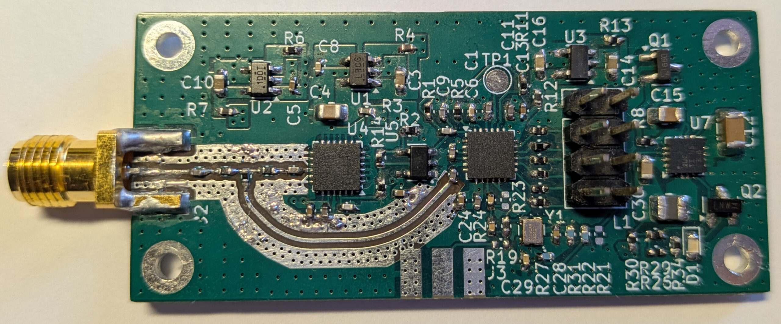
I designed a small PCB with an ADF4158 and HMC391, which I now have built and tested. In this post I explain some of the aspects of the board design and the results of the initial tests.
Board design
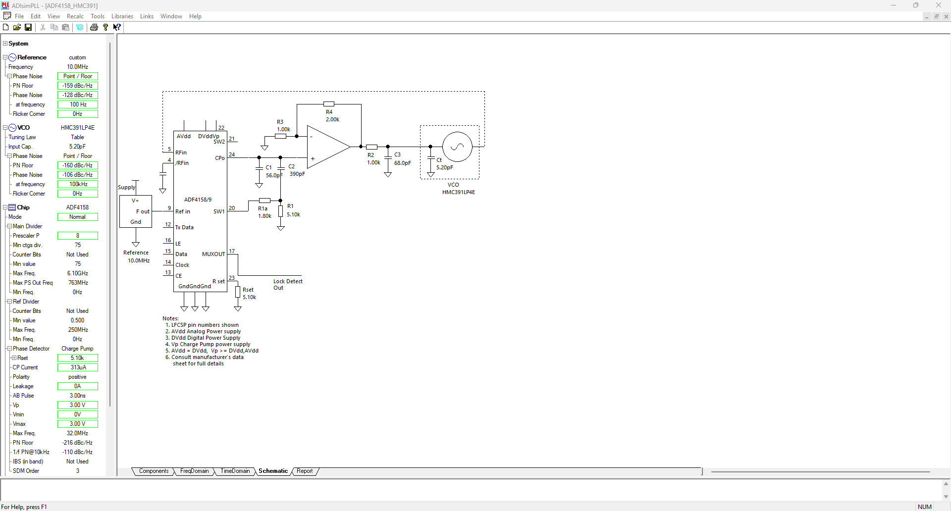
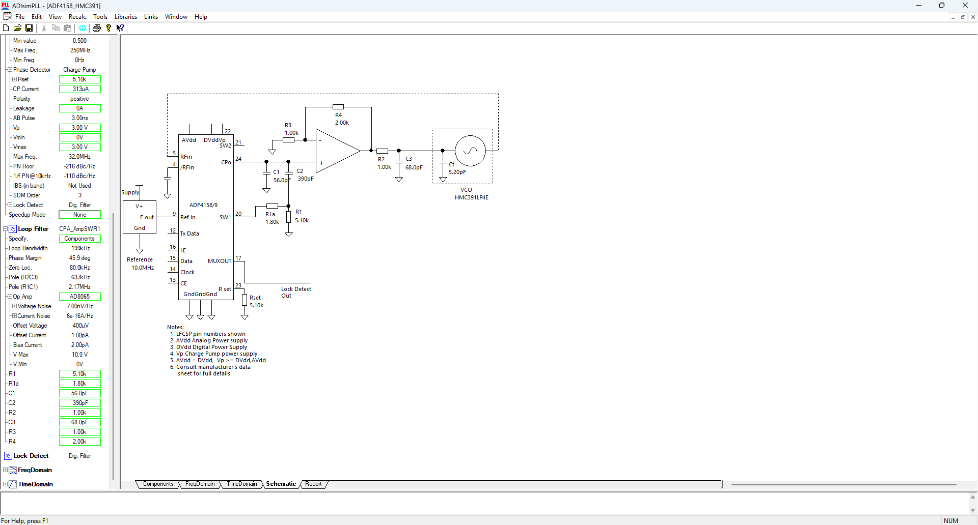
The main aspect of the schematic design is the VCO loop filter. I have used ADIsimPLL to design and simulate it. The HMC391 uses a tune voltage of 0-10 V, so an active loop filter with an op amp is needed. After looking around for options included in the ADIsimPLL library, I decided to use the AD8065 since it is a single-supply rail-to-rail op amp that has a reasonable noise performance for its cost.
The loop filter needs to be designed in terms of the loop filter bandwidth. Since I wanted this board to be also useful for non-radar applications that use a constant-frequency LO, I didn’t want to set the bandwidth too high, as that would degrade phase noise. So I played around with some time-domain simulations to find a reasonable value.
Since part of the intention of this project is to experiment with different FMCW waveforms, I thought of some extreme parameters. The frequency sweep of the chirp would be from 4.2 GHz to 4.45 GHz, giving 500 MHz bandwidth at 10 GHz. In the most extreme case, I might want to resolve Doppler non-ambiguously up to 250 m/s, if for instance I want to try this radar with commercial airliners. At 10.25 GHz that corresponds to a Doppler of 8.5 kHz, so the chirp duration should be at most 60 usec to avoid chirp-to-chirp frequency ambiguities. On the other hand, 60 usec corresponds to a round-trip-time for a target at 9 km distance, and FMCW requires the round-trip-time to be smaller than half of the chirp duration for best results. So realistically, observing aircraft with FMCW probably benefits from a much longer chirp duration determined in terms of the maximum range even though this would give ambiguous Doppler. In any case, this 60 usec chirp duration gives a good extreme case to design the loop filter around.
Looking at the lock time for a frequency jump from 4.45 GHz to 4.2 GHz, which would happen in a sawtooth chirp, I decided on a 200 kHz loop filter bandwidth. Intuitively this makes sense, because the reciprocal of 200 kHz is 5 usec, which is reasonably small compared to a 60 usec chirp duration.
The following two screenshots show the design of the loop filter in ADIsimPLL. The only difference between the two of them is that in the second one I have scrolled down on the left panel so the loop filter parameters can be seen.
The frequency domain simulation gives a reasonable phase noise.
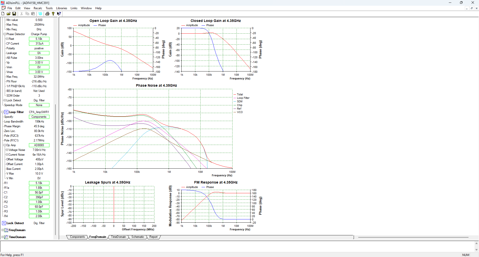
In the time domain simulation, I have first simulated a sawtooth that covers 4.2-4.45 GHz with a period of 51.2 usec. In order to leave time for the loop filter to jump from 4.45 GHz to 4.2 GHz, I have used the ramp delay feature to delay the start of the ramp by 10 usec, which is enough time to reduce the frequency error to something reasonable.
However, there is a problem with this design. The loop overshoots by almost 100 MHz when jumping in frequency. This is a problem, because it means that if we want to fit our radar waveform in 10-10.5 GHz, we need to dedicate the lower 200 MHz to this overshoot, which is a waste of bandwidth. Experimenting more after having built the board has shown me that the overshoot can be improved a lot by tweaking the phase margin of the loop filter. Therefore, I will need to redesign the loop filter if I want to get optimal results with a sawtooth. I’m not too concerned about this, since changing the loop filter only requires changing three capacitors and two resistors, which is easy to do.
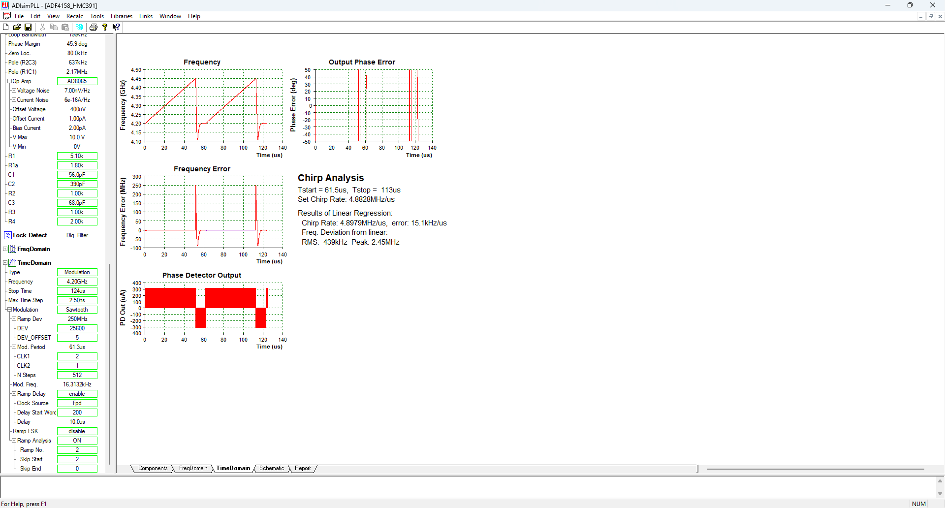
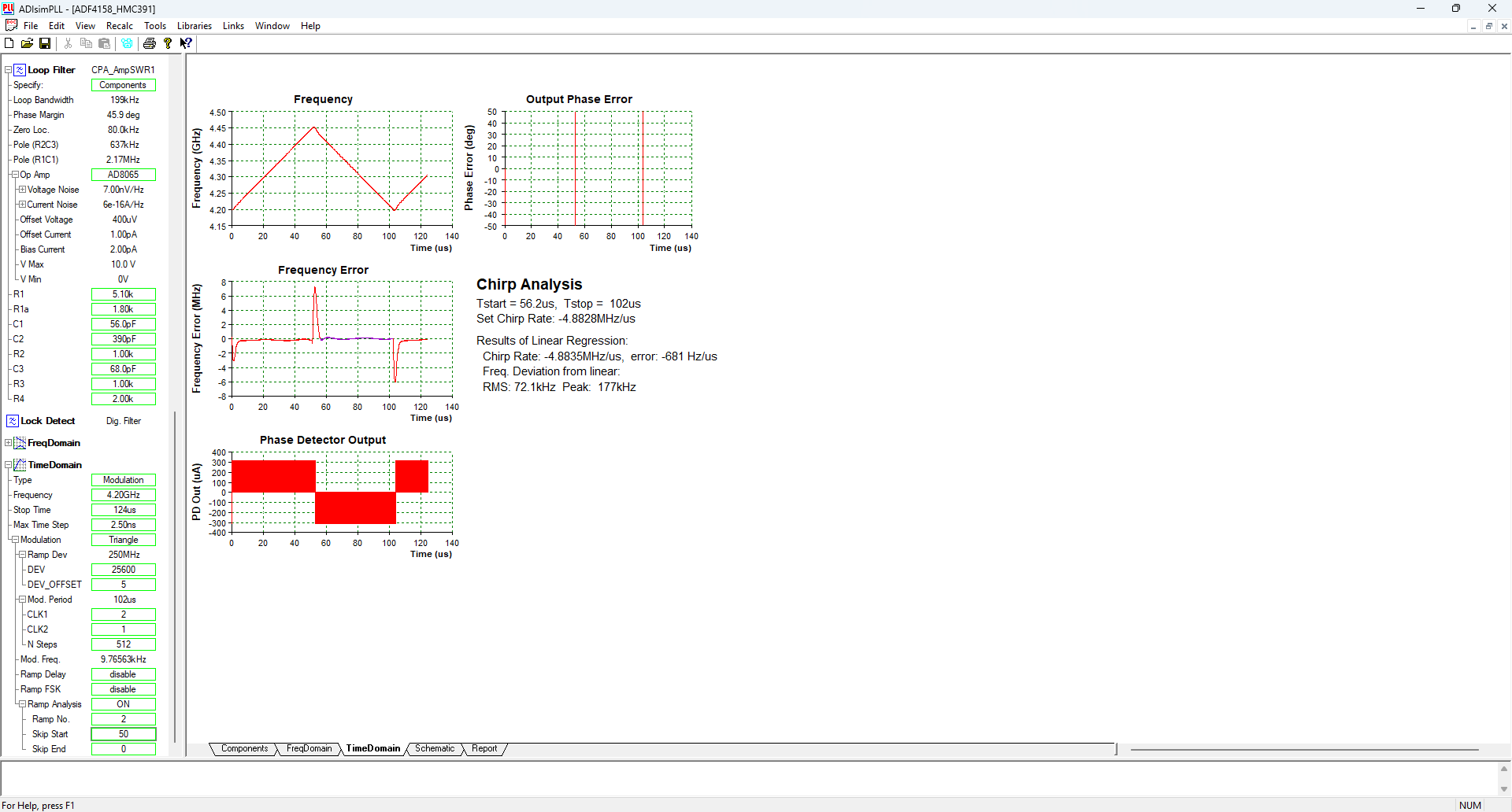
On the other hand, a triangle wave works quite reasonably, since there are no abrupt jumps in frequency. There is just a few MHz of error at the corners of the triangle.
The main section of the PCB schematic is very similar to the schematic shown in ADIsimPLL. There is a 10 MHz oscillator and an external reference option used as the ADF4158 reference. The output of the HMC391 goes to a -6 dB resistive splitter, with one of the paths going to the ADF4158 RFINA feedback, and the other being the RF output of the board.
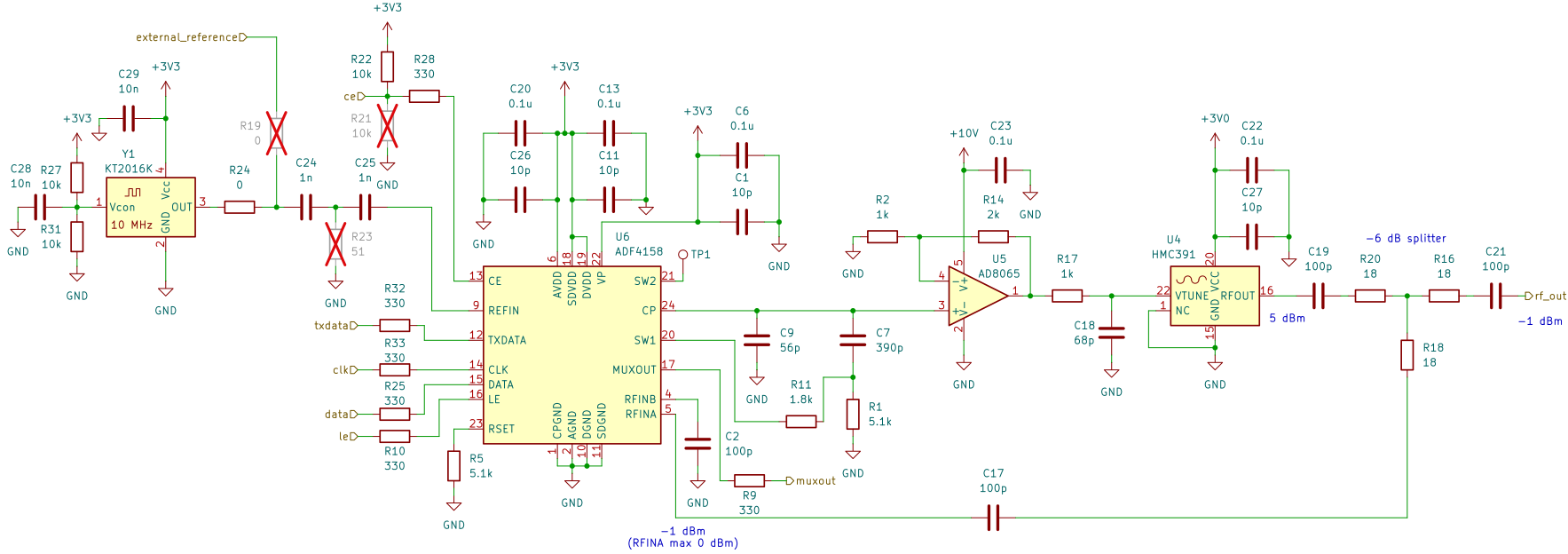
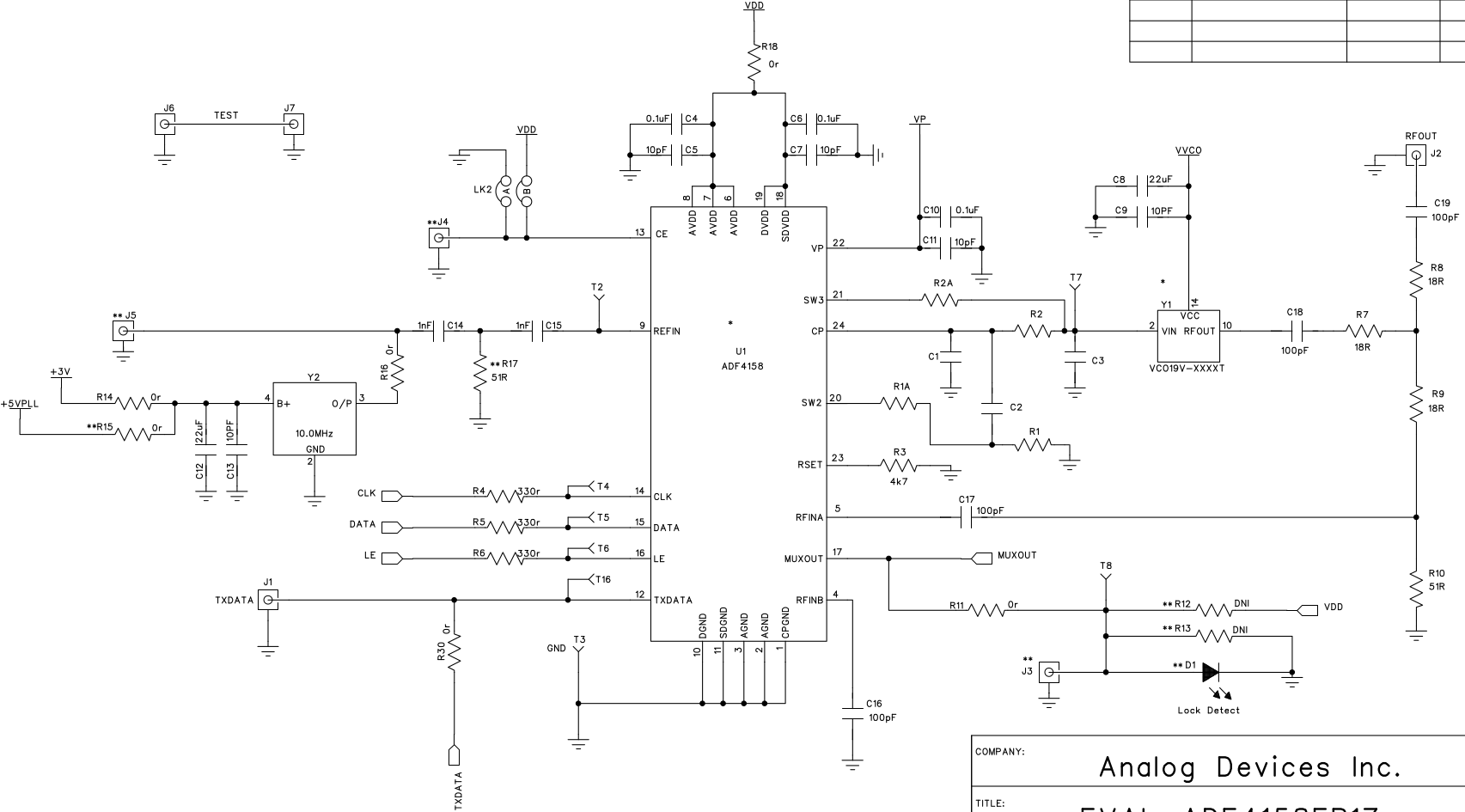
This design is heavily inspired by the EVAL-ADF4158 evaluation board. The main difference is the choice of VCO. However, there is a resistor R10 in the eval board that looks strange. It loads RFINA with an additional 50 ohms (RFINA is supposed to be a 50 ohm input), and it is not at all clear why R10 is present. Discussing this with other people, this R10 might have been a mistake, so I left it out of my design. Henrik Forstén has an FMCW radar design based on the ADF4158 and he has also omitted R10.
The remaining part of the schematic is the power supplies for all the components. The input is 12-16 V (nominally 12V). A linear regulator generates 10 V for the op amp that drives the VCO control voltage. A switching regulator produces 5 V, and then linear regulators are used to obtain 3.3 V and 3 V. The HMC391 uses a nominal Vcc of 3 V. Although according to the datasheet it can probably work at 3.3 V, but I didn’t want to risk it, and provided a dedicated 3 V regulator for the VCO. The ADF4158 and the 10 MHz oscillator run at 3.3 V. The full schematic can be seen here.
I wanted the PCB to be inexpensive to fabricate, since part of the motivation of this project is to help other people experiment with FMCW radar, since the ADALM-PHASER is just too expensive for hobbyist use. I wanted to fabricate in JLCPCB. After trying a two-layer design with a rather thin FR4 PCB and asking other people, I decided to go for a four-layer design using a particular JLCPCB FR4 stackup (JLC04161H-7628) that gave 50 ohm trace dimensions reasonably well adapted to a 0402 component size.
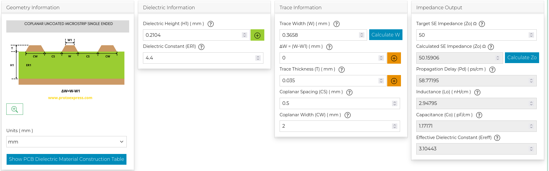
The JLC04161H-7628 has the following stackup according to the controlled impedance information at JLCPCB. The 7628 prepreg has a dielectric constant of 4.4.
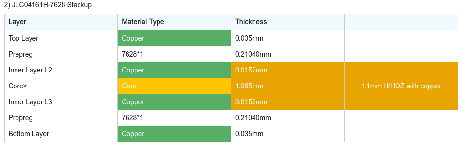
Using the impedance calculator from Sierra circuits, I designed a coplanar waveguide between the top layer and the first inner layer with a coplanar spacing of 0.5 mm. This gives a trace width of 0.3658 mm. For comparison, 0402 components have a width of 0.5 mm, so the match between the trace width and the passive components is not exact, but it is reasonably close.
The PCB has most of the routing, including all the RF routing on the top layer. All the components are mounted on the top side of the board. Inner layer 1 is a ground plane, which also acts as ground plane for RF traces. Inner layer 2 contains polygon pours for several of the power nets, but the rest is also used as ground plane. The bottom layer is also a ground plane.
The board size is 55×25 mm, which is what felt right once I had laid out all the components. There is an SMA connector for the RF output and an optional RF connector for an external reference that is expected to be populated only in rare cases. When I manufactured the boards at JLCPCB, the cost was $7.10 for 5 PCBs and $13.20 for 10 PCBs, which seems quite inexpensive to me. The BOM cost is around 50€.
I assembled the PCB by hand, soldering the QFN components and the oscillator with hot air and the rest of the components with a soldering iron. Most of the passives are 0402, because I like soldering tiny things. If other people are interested in building this project, then it is probably worth to explore PCBA options, since I understand that not everyone can (or wants to) solder a board like this by hand.
Software
To program the ADF4158, I have used a Longan Nano board that I had around. This is just because I already had this board and because it has a RISC-V microcontroller, which is cool. I have written the software in Rust. It can be found in the following repository. This software should be easy to adapt to any board or microcontroller that has some Rust support. Three GPIOs are used to write into the ADF4158 registers (which needs lines for clock, data and latch enable). To test different cases, I have included the following three configurations in the software:
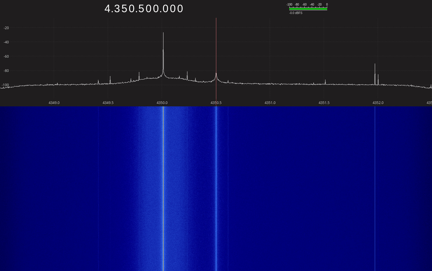
- CW signal at 4.35 GHz.
- Sawtooth covering 4.2-4.45 GHz with a period of 51.2 usec (as in the ADIsimPLL simulation above). This has approximately 100 MHz of overshoot as in the simulation.
- Triangle covering 4.2-4.45 GHz with a period of 102.4 usec. The frequency range for the triangle is slightly less than 4.2-4.45 GHz so that the occupied bandwidth is within 4.2-4.45 GHz.
The configuration can be selected and applied by connecting one of three GPIOs to ground. This gives an easy way of changing configurations.
Iterative development with this software is very simple. After doing some changes, I just need to press the BOOT and RESET buttons on the Longan Nano to get it into the bootloader and then run just flash on the software project to build it and flash it.
Testing
To test the board, I am powering it with a lab power supply at 12 V, connected the RF output to a USRP B205mini through 50 dB of attenuation, and I am using the Longan Nano to configure the ADF4158. Before the ADF4158 is configured, the board draws 22 mA. After the ADF4158 is configured, the current draw increases to 33 mA.
The following screenshot shows the CW output at 4.35 GHz in GQRX. In all these tests the RX gain of the USRP has been set to 60 dB.
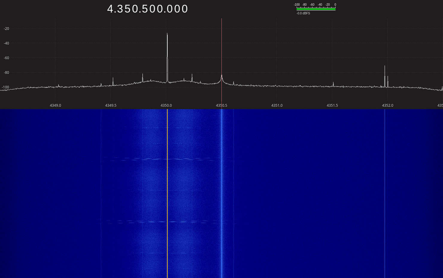
We can see that occasionally some X patterns appear in the waterfall. These can be seen better in the following Inspectrum screenshot. They happen periodically every 3.4 seconds approximately, and there are also some weaker spurs with a similar pattern and periodicity.
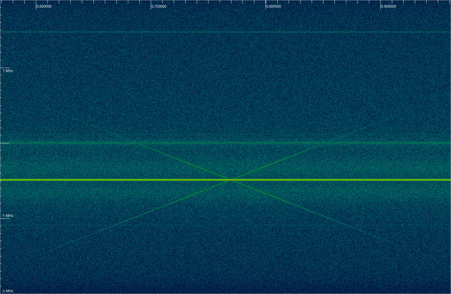
I don’t know what causes these spurs. I have played with the ADF4158 settings and I have found that they frequency with which they appear depends on the fractional word of the PLL and that by enabling the negative bleed current the spurs disappear, although phase noise becomes slightly worse.
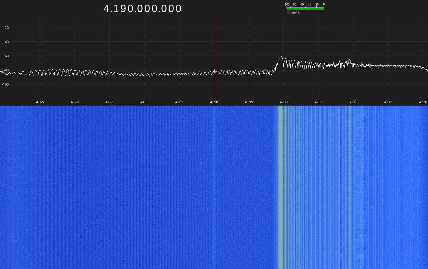
The sawtooth and triangle configurations cover a bandwidth of 250 MHz, so the USRP doesn’t have enough bandwidth to look at the full waveform. Still, we can look at the edges of the occupied bandwidth to see if the synthesizer is working correctly. For instance, the following GQRX screenshot shows that the triangle wave fits nicely into the occupied bandwidth, which is supposed to be 4.2 – 4.45 GHz (the triangle sweep technically starts at 4.205 GHz).
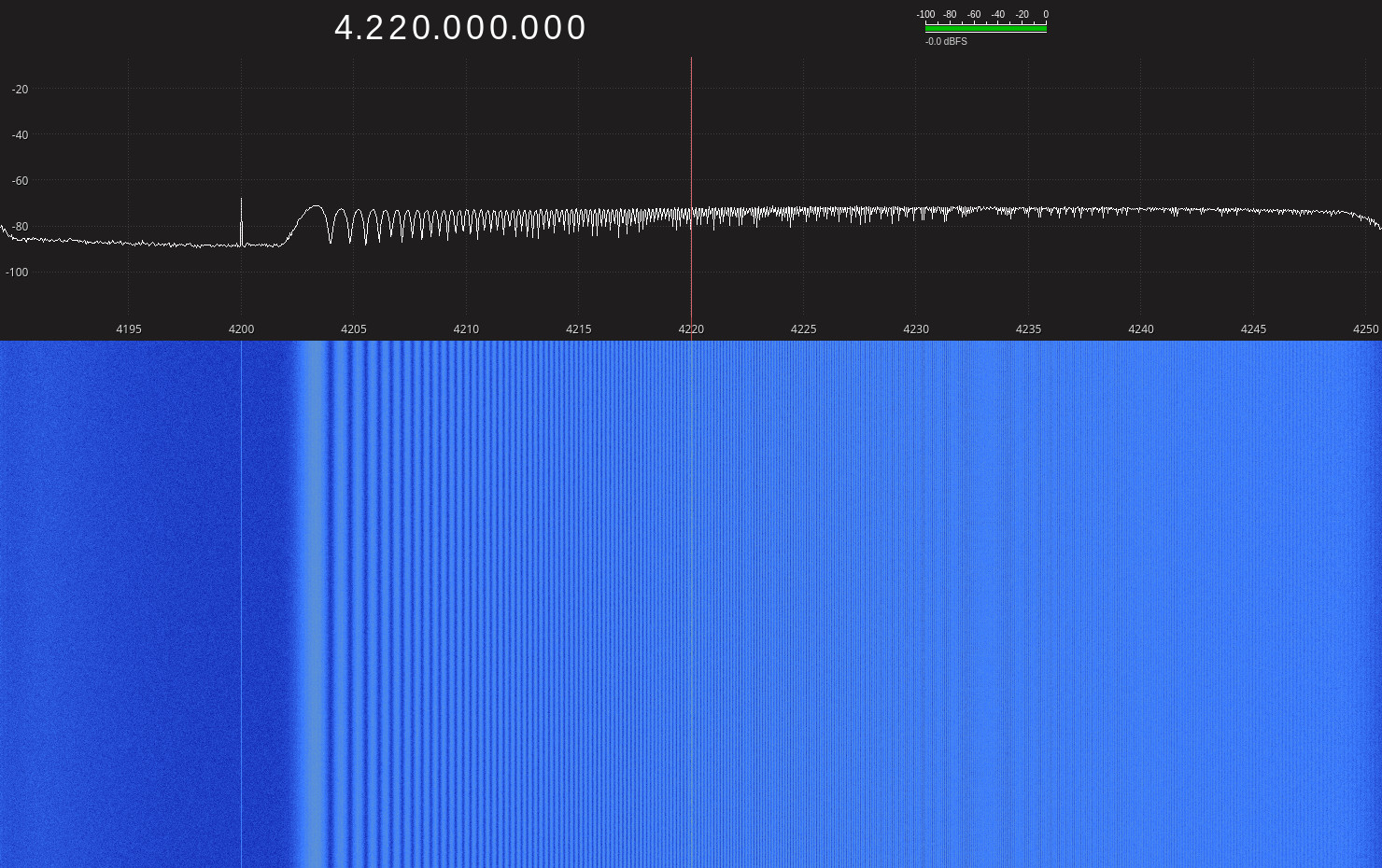
The same signal in Inspectrum shows a behaviour in the corners of the triangle wave that is similar to the simulation. We can measure that the period matches the 102.4 usec that we expect.

A good way to measure the full waveform is to probe the output of the loop filter op amp with an oscilloscope. This output almost equal to the HMC391 VCO control voltage, and it is low impedance, so the filter is not disturbed at all by a 10x probe. The voltage to frequency transfer function with the HMC391 is slightly non-linear, but still looking at the voltage gives a good idea about the frequency versus time curve of the waveform.

With the sawtooth configuration we can see that there is a significant amount of noise below 4.2 GHz. This is due to the overshoot that was predicted in the ADIsimPLL simulation.
Inspectrum shows better how the overshoot looks like, although the overshoot is large enough that it doesn’t fit in the 61.44 Msps sample rate that I’m using with the USRP.

The op amp output voltage gives a better view of the whole waveform including the overshoot.

The ADF4158 has an option to enable fast lock mode during the ramp delay period. In fast lock mode, the charge pump current is increased by a factor of 16 in order to make the loop bandwidth larger. To compensate for this, the loop damping resistor needs to be decreased by a factor of 1/4. There is a pin SW1 that gets connected to ground during fast lock mode. This allows changing the loop damping resistor by using two resistors in such a way that their combined value changes depending on whether SW1 is connected to ground or open. There is also a pin SW2 that gets connected to the charge pump pin during fast lock mode, but this pin is not used with active loop filter topologies.
However, I have found that in this case the fast lock mode oscillates wildly, to the point where the loop appears unstable in fast lock mode. This is shown in the figure below. From what I can tell by probing, all the circuit seems to be working correctly: the SW1 pin is shorted to ground during fast lock mode and current flows through the corresponding resistor.

ADIsimPLL does not support simulating ramp delay fast lock mode, but it supports simulating a frequency change with fast lock mode, and this oscillating behaviour does not happen. In the simulation, the overshoot is reduced to about 50 MHz and the lock time decreases significantly, but the shape of the curve is roughly the same.
Conclusions
The board that I have built with an ADF4158 and HMC391 is working correctly. A redesign of the loop filter could be done to improve performance with a sawtooth waveform, and perhaps to fix fast lock mode, but this only involves a change of passive components, and it is not critical for what I’m going to do next.
The PCB design can be found in the ADF4158_PCB repository, and the software is in the ADF4185_SW repository.