Some weeks ago, I presented at FOSDEM my work-in-progress high performance SDR runtime qsdr. I showed a hand-written NEON assembly implementation of a kernel that computes \(y[n] = ax[n] + b\), which I used as the basic math block for benchmarks on a Kria KV260 board (which has a quad-core ARM Cortex-A53 at 1.33 GHz). In that talk I glossed over the details of how I implemented this NEON kernel. There are enough tricks and considerations that I could make a full talk just out of explaining how to write this kernel. This will be the topic for this post.
Note: this post assumes familiarity with the aarch64 assembly syntax, particularly with the way that NEON registers are denoted depending on the context. For example, you should understand that v0.4s and q0 refer to the same 128-bit NEON register, and v0.2s and d0 denote the 64 LSBs of this same NEON register. It might be worth to review the syntax if this doesn’t make sense immediately to you.
Cortex-A53 characteristics
Something peculiar about the Cortex-A53 is that documentation explaining its instructing timing is not publicly available. There is, for instance, a Cortex-A57 Software Optimization Guide, but the equivalent document for the Cortex-A53 is not available. I believe that it exists, but it is only available under an NDA. Therefore, all the wisdom about how to optimize code for the Cortex-A53 is folklore coming from people that have either reverse-engineered instruction timings by performing micro-benchmarks, or which have had access to this NDA documentation. Here are some links that I have found quite useful when starting to understand how the Cortex-A53 works and what tricks can be used:
- Assembly still matters: Cortex-A53 vs M1
- ARM A53 and A55 dual-issue wiki from Tencent ncnn
- A thread about A53 dual-issue capabilities in the ARM forums
- 7-zip benchmarks for the Cortex-A53
Nevertheless, this documentation has not been sufficient to understand fully how this CPU works. I have written many instruction timing micro-benchmarks to verify the claims in these links and to test how other combinations of instructions work.
The Cortex-A53 is an in-order execution CPU with partial dual-issue capabilities. This means that machine code is always executed in order, but under some conditions two instructions can be issued in the same clock cycle and executed in parallel. The in-order execution property is quite interesting for my purposes. First, it makes instruction timing much easier to test and understand. Second, it makes the CPU less tolerant to bad code. An out-of-order CPU might outsmart the programmer by reordering code to avoid stalling, but an in-order CPU can show a huge difference between badly ordered code that keeps stalling and properly ordered code that avoids stalls as much as possible. Therefore, the potential benefits of understanding how the CPU works and optimizing the code by hand are much higher for in-order CPUs.
The following diagram refers to the Cortex-A57 rather than the Cortex-A53, but still can be useful for a preliminary understanding of how the A53 works. The A57 is the A53’s big brother (quite literally, since the two were designed to work as pairs in a big.LITTLE system). The A57 is an out-of-order CPU, but it has some commonalities with the A53.
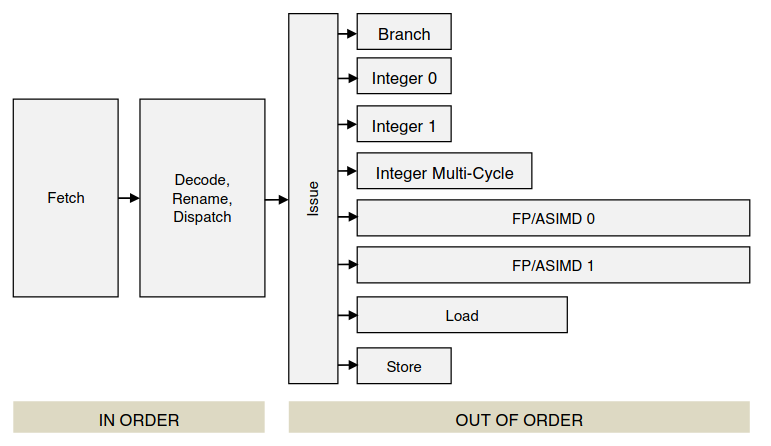
In the diagram we can see that the A57 has two execution units for integer arithmetic. This is also true for the A53. It can dual-issue and execute in parallel integer instructions which have no interdependencies, such as
add x0, x0, x0
add x1, x1, x1
(see the micro-benchmark).
Of more interest for this post are the two units marked as FP/ASIMD. These are used for floating-point and NEON instructions. There are some subtleties regarding these two units, and in fact they are not completely interchangeable (at least for the A57), but for our purposes the following mental model should be good enough. Each of the two NEON units works on a 64-bit half of a 128-bit NEON register. Executing a NEON instruction that works with a 128-bit register, such as
fadd v0.4s, v0.4s, v0.4s
takes up both NEON units, so no other instruction that uses NEON registers (even for load/store or data movement to/from a GPR) can be executed at the same time. However, generally speaking, two NEON instructions that only access the 64-bit half of independent NEON registers can dual-issue and execute in parallel. For instance, the following two instructions dual-issue and execute a 64-bit add of 2 floats and a 64-bit load in parallel.
fadd v0.2s, v0.2s, v0.2s
ldr d1, [x0]
(see micro-benchmark).
Another thing that is very important to understand is the width of the load and store data paths connecting the CPU to the L1d cache. This is documented in the Arm Cortex-A53 MPCore Processor Technical Reference Manual. The load data path is 64 bits, while the store data path is 128 bits. This asymmetry is quite interesting, and the fact that the load path is only half the width of a NEON register is an important limitation that gives rise to many tricks.
Storing a 128-bit NEON register is quite straightforward. An instruction such as
str q0, [x0]
takes one cycle to issue and can generally be dual-issued with other instructions that do not use NEON registers. Usually a sequence of these stores can be executed at a throughput of one instruction per cycle. Likewise, the multi-register stores such as
st1 {v0.4s-v3.4s}, [x0]
take one cycle per register. The advantage of these instructions is that they make the code smaller, but the disadvantage is that generally they cannot dual-issue with other instructions.
Loading a 128-bit NEON register efficiently is more complicated. The naïve
ldr q0, [x0]
takes two cycles to issue and doesn’t seem to dual-issue with other instructions. Probably this 128-bit load is decomposed by the CPU into two 64-bit load micro-instructions. Similarly, multi-register loads such as
ld1 {v0.4s-v3.4s}, [x0]
take two cycles per register. Loading values to fill up a 128-bit NEON register is always going to take two cycles worth of 64-bit loads, due to the load data path to the L1d cache. However, to improve performance we generally want these 64-bit loads to happen at the same time that the CPU is doing other useful work. This is the source of many possible tricks, some of which will be explained below.
A final remark about the A53 characteristics is that it seems to have only one AGU (address generation unit). Therefore, at any given cycle only a store or a load can be issued. It doesn’t seem possible to dual-issue a store and a load (or two 64-bit stores).
A word about llvm-mca
llvm-mca is a tool from the LLVM project that uses LLVM’s instruction timing models to determine and represent how a piece of machine code is executed by a given CPU. This is a great tool to learn about the specifics of different CPUs, and to optimize code. However, for the Cortex-A53, llvm-mca gives quite wrong results even in many simple cases. This is due to the rather simplistic timing model that LLVM has for the Cortex-A53, which is in fact justified by the lack of suitable public documentation mentioned above.
This has two consequences. First, llvm-mca shouldn’t be used to learn about how the A53 works, since it is most likely to be misleading rather than helpful. Second, any compiler that is using LLVM to optimize machine code (such as the Rust compiler or clang) will not do very well for the A53, since it’s essentially trying to optimize code using a wrong CPU model. Therefore, there is potentially much to gain by writing assembly by hand.
Here are some particular problems with llvm-mca, shown in Compiler Explorer:
- It believes that
ldr q0, [x0]has a throughput of one instruction per cycle - It believes that a NEON
faddand a integeraddcannot dual-issue, and moreover theaddneeds to stall so that it can retire at the same time as thefadd(which does not make any sense) - It does not know that a 64-bit NEON
faddand a 64-bitldrto an unrelated NEON register can dual issue, and moreover it believes that theldrneeds to stall so that it can retire at the same time as thefadd
Theoretical analysis of maximum performance
With the information I have already given about the Cortex-A53, we can already give an upper bound on how fast a kernel like \(y[n] = ax[n] + b\) (where all the variables here are float32) can be executed. Later we will see how to write code that achieves this theoretical bound asymptotically as the number of iterations grows to infinity (assuming all the data is in L1d cache when needed).
First, let’s speak about the math itself. There are essentially two different ways in which we can implement the operation \(ax[n] + b\). We can perform the product \(ax[n]\) with a NEON fmul and then the sum \(ax[n] + b\) with a NEON fadd. Naïvely, this would be something like:
fmul v0.4s, v0.4s, v31.s[0]
fadd v0.4s, v0.4s, v30.4s
This assumes that four \(x[n]\) values are loaded in v0.4s, that v31.s[0] contains the constant \(a\) and v30.4s contains four copies of the constant \(b\) throughout the whole execution of the kernel (unlike fmul, the fadd instruction is not available in a form that uses a single scalar v30.s[0]). The result \(y[n]\) is placed back into v0.4s. This code shown above is very bad for performance, because the fadd needs to stall for three cycles to wait for the result of the fmul to be available, but my main point here is to explain how the math will be calculated. Arranging things to avoid stalls due to pipeline latency will be done later.
The second option is to use the fmla instruction to perform the whole \(ax[n] + b\) operation. Naïvely this looks quite promising, but unlike in x86-64, where FMA stands for fused-multiply-add, in aarch64 FMA stands for fused-multiply-accumulate. The difference is that an x86-64 FMA has 4 registers: a destination register and the registers for the 3 operands, while in aarch64 FMA has only 3 registers, because the destination register and the register for the operand \(b\) must be the same (this is where “accumulate” comes from). Therefore, to implement our \(ax[n] + b\) operation we would need two instructions: one to load the accumulator register with \(b\), and another one to perform the fmla. This would look like so:
mov v1.4s, v30.4s
fmla v1.4s, v0.4s, v31.s[0]
As in the fmul and fadd approach, four \(x[n]\) values are in v0.4s, and v31.s[0] and v30.4s contain respectively \(a\) and four copies of \(b\). The result is placed in v1.4s.
[Edit: dzaima mentioned in Mastodon that a 4-register FMA instruction only existed in a few AMD CPUs. Regular x86-64 FMA instructions use only 3 registers. However, the remark above is still more or less true, because in x86-64 the vfmadd132ps instruction can be used to calculate \(ax[n]+b\) and place the result in the register that contains \(x[n]\), while in aarch64 the only possibility is to use fmla, which places the result in the register that contains \(b\). The following Compiler Explorer example illustrates the difference that this makes.]
Both approaches take the same number of instructions and the same number of cycles to run. The main difference is in rounding. Since fmla is performing the multiplication and sum in the same instruction, it can in principle give a more accurate result by not discarding some bits that would be rounded by fmul. However, for simplicity I will use fmul and fadd throughout this post.
We have established that in any case evaluating \(y[n] = ax[n] + b\) needs two NEON operations (even if one of them is mov). Thus, no matter what we do, calculating two \(y[n]\) results will require usage of one of the two NEON execution units in two clock cycles.
The next thing we need to evaluate is moving data in and out of the CPU. No matter how we do this, the \(x[n]\) data needs to be written into the NEON registers at some point and the \(y[n]\) data needs to be read out of the NEON registers at some point. Remember that moving data to/from the NEON registers also uses the NEON execution units. So loading two \(x[n]\) values will at least require usage of one of the two NEON execution units in one clock cycle, and storing two \(y[n]\) values will at least require usage of the two NEON execution units in one clock cycle.
Therefore, to compute two \(y[n]\) values we need to keep one of the two NEON execution units busy for four cycles (one for load, one for fmul, one for fadd, one for store, if following the first approach). Since there are two NEON execution units, we can compute four \(y[n]\) values over the course of four cycles. Therefore, the maximum theoretical throughput is one calculation of \(y[n] = ax[n] + b\) per clock cycle. This is a throughput of 2 FLOPs/cycle, which is not too bad taking into account that for this very simple math kernel there is a lot of overhead due to data movement.
Dealing with the 64-bit load data path
A naïve implementation informed by the theoretical considerations, and forgetting for a moment about result latency, might look like the following.
ldr q0, [x0]  # load 4 x[n] values
fmul v0.4s, v0.4s, v31.s[0]  # perform 4 a*x[n]
fadd v0.4s, v0.4s, v30.4s    # perform 4 a*x[n] + b
str q0, [x1]  # store 4 y[n] values
We would hope to run this at one instruction per clock cycle in order to achieve the maximum theoretical throughput of one \(y[n]\) per clock cycle. However the problem is that due to the 64-bit load data path the ldr takes two clock cycles instead of one. As I mentioned above, performing a 128-bit load is generally a bad idea, since we are wasting a cycle in which the CPU could do other useful work.
Perhaps somewhat counter-intuitively, there is a solution to this problem which consists in matching all that we do to the 64-bit load data path. Rather than operating on 128-bit vectors composed of four float32‘s, we operate on 64-bit vectors composed of two float32‘s. The partial dual-issue characteristics of the Cortex-A53 is what makes this approach viable. The key is that we can use one of the two NEON execution units to move data in or out of a 64-bit NEON register while the other NEON execution unit is performing a math operation on another 64-bit register. Forgetting again to address result latency, this approach is as follows.
# assume v0.2s already contains 2 x[n] values
# from a previous iteration

fmul v0.2s, v0.2s, v31.s[0]
str d1, [x1]  # store 2 y[n] results of previous iteration

fadd v0.2s, v0.2s, v30.2s
ldr d1, [x0]  # load 2 x[n] values

fmul v1.2s, v1.2s, v31.s[0]
str d0, [x1, #8]  # store 2 y[n] results of previous iteration

fadd v1.2s, v1.2s, v30.2s
ldr d0, [x0, #8]  # load 2 x[n] values
The instructions in this listing are grouped in pairs that dual-issue, so it takes 4 cycles to run this code. We can see that we are calculating and storing four \(y[n]\) outputs in these 4 cycles. This code is supposed to run in a loop (perhaps unrolled if needed), and the x0 and x1 addresses would need to be incremented in each loop iteration somehow. But the main point of this code is that the first two pairs of instructions calculate the math for two \(y[n]\)’s at the same time that two \(y[n]\)’s from the previous iteration are stored and two \(x[n]\)’s for the next block are loaded. The second two pairs of instructions calculate the math with the two \(x[n]\)’s that were just loaded, and simultaneously store the two \(y[n]\)’s just calculated and load the two \(x[n]\)’s for the next loop iteration.
As mentioned, this code does not take into account result latency. The fadd instructions would stall for several cycles, since they need to wait for the result of the fmul to be available. Likewise, the fmul would stall until the result of ldr is available, and the str would stall to wait for the result of the fadd. This problem has a mechanical solution in most situations, which is to send more independent operations into the pipeline to hide the result latency. This is best explained with an example. Rather than doing
fmul v0.2s, v0.2s, v31.s[0]
fadd v0.2s, v0.2s, v30.2s
we can do something like
fmul v0.2s, v0.2s, v31.s[0]
fmul v1.2s, v1.2s, v31.s[0]
fmul v2.2s, v2.2s, v31.s[0]
fmul v3.2s, v3.2s, v31.s[0]
fadd v0.2s, v0.2s, v30.2s
fadd v1.2s, v1.2s, v30.2s
fadd v2.2s, v2.2s, v30.2s
fadd v3.2s, v3.2s, v30.2s
This assumes that suitable inputs \(x[n]\) have already been loaded into v0.2s, v1.s2, v2.2s, and v3.2s. The trick here is that by the time that the first fadd executes, the first fmul has already finished and its results are available, and likewise for the other dependant fmul/fadd pairs. In fact, in the Cortex-A53 both fmul and fadd have a result latency of 4 cycles, so pipelining four independent fmul or fadd instructions is the typical approach to hide result latency.
Applying this pipelining trick to the code above, we obtain the following.
fmul v0.2s, v0.2s, v31.s[0]
str d4, [x1, #8]
fmul v1.2s, v1.2s, v31.s[0]
str d5, [x1, #16]
fmul v2.2s, v2.2s, v31.s[0]
str d6, [x1, #24]
fmul v3.2s, v3.2s, v31.s[0]
str d7, [x1, #32]!

fadd v0.2s, v0.2s, v30.2s
ldr d4, [x0, #8]
fadd v1.2s, v1.2s, v30.2s
ldr d5, [x0, #16]
fadd v2.2s, v2.2s, v30.2s
ldr d6, [x0, #24]
fadd v3.2s, v3.2s, v30.2s
ldr d7, [x0, #32]!

fmul v4.2s, v4.2s, v31.s[0]
str d0, [x1, #8]
fmul v5.2s, v5.2s, v31.s[0]
str d1, [x1, #16]
fmul v6.2s, v6.2s, v31.s[0]
str d2, [x1, #24]
fmul v7.2s, v7.2s, v31.s[0]
str d3, [x1, #32]!

fadd v4.2s, v4.2s, v30.2s
ldr d0, [x0, #8]
fadd v5.2s, v5.2s, v30.2s
ldr d1, [x0, #16]
fadd v6.2s, v6.2s, v30.2s
ldr d2, [x0, #24]
fadd v7.2s, v7.2s, v30.2s
ldr d3, [x0, #32]!
Each pair of instructions in this listing can dual-issue, so it takes 16 cycles to run all this code (which is supposed to be run in a loop). A total of 16 outputs \(y[n]\) are computed and stored. Instructions with data dependencies are placed at least 4 cycles apart, so the results are always ready and the CPU doesn’t stall.
In the first block, the multiplications on registers v0.2s-v3.2s are performed assuming that the corresponding \(x[n]\)’s were loaded in a previous loop iteration. The registers d0-d3, containing the results from the previous loop iteration are stored at the same time. In the second block, the additions on registers v0.2s-v3.2s are performed, and simultaneously registers d0-d3 are loaded with new \(x[n]\) values for the next blocks. The next two blocks are the same as the first two, but with the roles for the registers d0-d3 and d4-d7 swapped.
Another neat trick that has appeared in this code is the pre-increment in some of the stores and loads, such as
str d7, [x1, #32]!
This updates the addresses x0 and x1 by incrementing them by 32 at the end of each block, without needing an extra instruction. The caveat is that the offsets all need to match this #32 (if writing this code naïvely the offset in this instruction would be #24 instead), so the first store/load has an offset of #8 instead of an offset of zero. This means that initially the addresses x0 and x1 need to point 8 bytes before the intended read/write locations. This is not a problem, as it is easy to account for before starting to run the kernel.
The code shown here works as intended, as demonstrated by its micro-benchmark. However, the problem is that it is already using all the dual-issue “slots” (i.e., all the instructions are arranged to dual-issue in pairs, and breaking this would require more clock cycles). Therefore, we don’t have freedom to add more instructions at zero cost. To turn this code into a real kernel that can be run on buffers of a size given at runtime, we need some additional instructions to calculate conditions and branch. This will come at extra cost for this approach. Perhaps for fixed-sized buffers which are not too large unrolling this loop would be a viable approach, but in general there is a better approach. The problem here comes from the fact that we are using 64-bit NEON arithmetic instructions, instead of 128-bit ones. Therefore, we need more instructions to perform the same work, although the code we obtain is relatively simple. Trying to make use of 128-bit instructions as much as possible gives a more efficient but more complex approach.
Matching the 64-bit load path to the 128-bit arithmetic and store paths
We begin this approach by coming back to the most naïve implementation:
ldr q0, [x0]
fmul v0.4s, v0.4s, v31.s[0]
fadd v0.4s, v0.4s, v30.4s
str q0, [x1]
The problem with this implementation is that the ldr was a bad idea because it takes two clock cycles. What we need to do to improve this approach is to find a way to perform a 128-bit load as two separate 64-bit loads at the same time that we perform other useful work. I learned the main tricks that I will use here in the Tencent ncnn wiki.
The key idea is that if we want to load values into several registers, say q0, q1, q2, q3, we can do so in the following rather roundabout way (which for the time being ignores result latency):
ldr x0, [x5, #8]

ldr x1, [x5, #24]

ldr x2, [x5, #40]

ldr x4, [x5, #48]

ldr x3, [x5, #56]

ldr d1, [x5, #16]
ins v3.d[1], x3

ldr d2, [x5, #32]
ins v1.d[1], x1

ldr d0, [x5]
ins v2.d[1], x2

ins v3.d[0], x4
ins v0.d[1], x0
The way to understand this piece of code is that to load 128 bits into the NEON register q1, at some point we can do ldr d1, [x5, #16] to load the 64 LSBs. After this, assuming that the corresponding data has already been loaded into a GPR x1, we move the data into the 64 MSBs of the NEON register by performing an ins v1.d[1], x1. The ins must be performed after the ldr, because the ldr clears the 64 MSBs. The key here is that these two instructions ldr and ins can dual-issue as long as they use different registers. What happens is that one NEON execution unit is being used for the 64-bit load, while the other NEON execution unit is being used for the 64-bit GPR to NEON register move.
Since for each particular register the ins must come after the ldr, for one of the four registers to load we are forced to perform two ins instead of an ldr, as otherwise we would need an extra cycle for the ins. In this way, we have the four last blocks of the listing, which are four pairs of instructions that dual-issue, and hence run in four clock cycles. They manage to load/move the data into the registers q0-q3 assuming that the 5 GPRs x0-x4 were already loaded with the required data. These 5 GPRs are loaded with regular GPR ldr‘s, which account for the first five lines of the listing. These 5 ldr‘s are shown here standalone, but the important thing about them is that they can dual-issue with many other kinds of instructions, as long as they are not load/stores (because there is only one AGU in the CPU). In particular, they can dual issue with the fmul and fadd instructions that we need to use for the math, so these ldr‘s execute for free.
An implementation using this load strategy and taking into account result latency looks like this.
# assume v0.4s-v3.4s are already loaded with x[n]'s
# and that v4.4s-v7.4s already have results y[n]

fmul v0.4s, v0.4s, v31.s[0]
ldr x0, [x5, #136]
fmul v1.4s, v1.4s, v31.s[0]
# empty dual-issue slot
fmul v2.4s, v2.4s, v31.s[0]
ldr x1, [x5, #152]
fmul v3.4s, v3.4s, v31.s[0]
ldr x2, [x5, #168]
fadd v0.4s, v0.4s, v30.4s
ldr x3, [x5, #184]
fadd v1.4s, v1.4s, v30.4s
ldr x4, [x5, #176]
st1 {v4.4s-v7.4s}, [x5] # 4 cycles to run
# no dual-issue possible
ldr d5, [x5, #144]
ins v7.d[1], x3
ldr d6, [x5, #160]
ins v5.d[1], x1
ldr d4, [x5, #128]!
ins v6.d[1], x2
ins v7.d[0], x4
ins v4.d[1], x0
fadd v2.4s, v2.4s, v30.4s
# empty dual-issue slot
fadd v3.4s, v3.4s, v30.4s
# empty dual-issue slot
This piece of code assumes that inputs \(x[n]\) are already loaded in registers v0.4s-v3.4s, and that registers v4.4s-v7.4s already contain results \(y[n]\) that need to be stored. The code computes the outputs \(y[n]\) for the inputs \(x[n]\), leaving them in registers v0.4s-v3.4s. It also stores the values in v4.4s-v7.4s and overwrites these registers with new inputs \(x[n]\).
This code should be followed by a similar piece of code which interchanges the roles of v0.4s-v3.4s and v4.4s-v7.4s. This similar piece of code uses a different pointer register x6 instead of x5. This allows the two blocks of code to be as symmetric as possible (so both of them contain a pre-increment instruction like ldr d4, [x5, #128]!, for instance), and also gives more freedom for prefetching (see below). Generally, the two pointers x5 and x6 differ by 64 bytes, and are initialized appropriately before this code begins executing. The use of two pointers is the reason why the pre-increment instructions use an offset of 128 bytes instead of 64 bytes.
The code takes 16 clock cycles to run, and 16 new results are computed, so the throughput matches the theoretical maximum of one result per cycle. There are a few places where an instruction could be added for free in an empty dual-issue slot. The store is done with a 4 register st1 instruction, since there is no drawback in doing that (it still runs at one store per clock cycle, albeit we lose the possibility of dual-issuing with these stores), and it is good for code compactness and perhaps to hint the CPU about write-combining and cache management.
Another feature in this code is that it is written as an in-place kernel (the results \(y[n]\) are written back to the same buffer from where the inputs \(x[n]\) are read from). Therefore, there is a single register x5 containing a pointer, which in this code points to the location where the first store (in memory order, not in program order) should be done. The pre-increment trick is used to update the pointer x5 for free. Some care should be taken to avoid using x5 for a few cycles after it is pre-incremented, since otherwise it would cause a stall. This is the reason why two fadd are placed at the end rather than before the st1.
There is some freedom to place the GPR ldr‘s, as evidenced by the presence of an empty dual-issue slot near the beginning of the code. The way in which these ldr‘s are placed is deliberate, since micro-benchmarking shows that other combinations cause some extra cycles. I believe that the reason is the A53’s limited capability for in-progress loads from L1d cache.
Writing a complete loop
The block of code from the previous section assumes that results \(y[n]\) are already present in v4.4s-v7.4s from a previous iteration, and inputs \(x[n]\) are already present in v0.4s-v3.4s from a previous iteration. It stores the results in v4.4s-v7.4s to memory, computes 16 new outputs \(y[n]\) using the inputs in registers v0.4s-v3.4s and stores them to memory, computes another 16 new outputs in registers v4.4s-v7.4, leaving them there to be stored in the next iteration, and loads new inputs \(x[n]\) in v0.4s-v3.4s for the next iteration. Moreover, it updates the pointers x5 and x6, by incrementing them by 128.
This code can be run in a loop in order to process any buffer whose length is a multiple of 128 bytes (32 floats). To convert the block of code into a loop, we need to check a loop termination condition and conditionally branch to the beginning of the block. The easiest way to determine the iteration in which the loop must end is to compare near the end of the loop the pointer x5 with an end-of-loop register x7 that contains the appropriate value of x5 at the final iteration, and which has been computed before the loop begins running. We use x5 instead of x6 for this comparison because x5 has been updated many instructions before the end of the block, so there is no chance for a data dependency stalling the comparison. We can add the comparison and branch instructions in the empty dual-issue slots of the last two fadd instructions of the loop. Therefore, the loop looks like this.
0:
// first half of the block
fmul v0.4s, v0.4s, v31.s[0]
ldr x0, [x5, #136]
// [...]
fadd v2.4s, v2.4s, v30.4s
# empty dual-issue slot
fadd v3.4s, v3.4s, v30.4s
# empty dual-issue slot
// second half of the block
fmul v4.4s, v4.4s, v31.s[0]
ldr x0, [x6, #136]
// [...]
fadd v6.4s, v6.4s, v30.4s
cmp x5, x7
fadd v7.4s, v7.4s, v30.4s
b.ne 0b
The number of cycles that this loop takes to run depends on how many iterations are done, because the branch predictor plays a role. For a small number of iterations, if this code is run frequently, the branch predictor can learn the pattern. For instance, for four iterations, the branch predictor can learn that the pattern is taken, taken, taken, not taken. In this case, the branch predictor is always right and the time to run the loop is 32 cycles per iteration, since the cmp and b.ne dual-issue with their preceding fadd and hence come at no extra cost.
For a larger number of iterations, which is the case we are mostly interested in, the branch predictor cannot learn the pattern and always guesses that the branch will be taken. This prediction only fails in the last iteration of the loop, incurring a branch prediction miss penalty of 7 cycles, because the CPU pipeline needs to be flushed. The overhead due to the branch prediction miss is not much. For instance, for processing 4096 floats, a total of 128 iterations are needed, which costs 4096 cycles plus 7 cycles of penalty. The penalty is only 0.17% of the cost.
Prologue and epilogue
The loop that we have is not a complete kernel, because it assumes that results are already in v4.4s-v7.4s and inputs are already in v0.4s-v3.4s. After the loop, it leaves these registers in the same situation. The loop can run as many iterations as needed in a pipelined manner, with each iteration using some of the work of the previous iteration and doing some work to enable the next iteration to run. But this pipeline must be started and flushed at some point. The kernel needs a prologue that starts loading the first inputs and computes the first results in v4.4s-v7.4s, so that the loop can start running in the state it expects. It also needs an epilogue that stores the results in v4.4s-v7.4s and that computes and stores the results corresponding to inputs in v0.4s-v3.4s.
For the prologue and epilogue I have decided to make the code reasonably simple, rather than spending much time trying to reduce the number of cycles they take to run. For a reasonably long buffer, the overhead of the prologue and epilogue is not much, so they are not so critical.
The prologue is as follows.
ld1 {v4.4s-v7.4s}, [x5]
fmul v4.4s, v4.4s, v31.s[0]
// empty dual-issue slot
fmul v5.4s, v5.4s, v31.s[0]
ldr x0, [x5, #72]
fmul v6.4s, v6.4s, v31.s[0]
ldr x1, [x5, #88]
fmul v7.4s, v7.4s, v31.s[0]
ldr x2, [x5, #104]
fadd v4.4s, v4.4s, v30.4s
ldr x3, [x5, #120]
fadd v5.4s, v5.4s, v30.4s
ldr x4, [x5, #112]
fadd v6.4s, v6.4s, v30.4s
// empty dual-issue slot
ldr d0, [x5, #64]
ins v3.d[1], x3
ldr d1, [x5, #80]
ins v0.d[1], x0
ldr d2, [x5, #96]
ins v1.d[1], x1
ins v3.d[0], x4
ins v2.d[1], x2
fadd v7.4s, v7.4s, v30.4s
// empty dual-issue slot
The first ld1 instruction takes 8 cycles to run, due to the 64-bit read data path to L1d. I have mentioned that using 128-bit load instructions is not a good idea, because each 128-bit load takes 2 cycles to run, and does not allow the CPU to do other useful work at the same time. Probably this prologue could be optimized somewhat by loading only the first 64 or 128 bits of inputs, and then starting to perform the fmul and fadd operations on them while the rest of the inputs are loaded. In this case, I have decided to keep the prologue simple. By spending 8 cycles to load the first inputs, we can then have some code that looks quite similar to the first block of the loop. Besides the ld1 and the instructions marked with an empty dual-issue slot comment, the remaining instructions can all dual issue. Therefore, this prologue takes 20 cycles to run.
The epilogue is very simple.
fmul v0.4s, v0.4s, v31.s[0]
fmul v1.4s, v1.4s, v31.s[0]
fmul v2.4s, v2.4s, v31.s[0]
fmul v3.4s, v3.4s, v31.s[0]
st1 {v4.4s-v7.4s}, [x5]
fadd v0.4s, v0.4s, v30.4s
fadd v1.4s, v1.4s, v30.4s
fadd v2.4s, v2.4s, v30.4s
fadd v3.4s, v3.4s, v30.4s
st1 {v0.4s-v3.4s}, [x6]
The two st1 instructions take each 4 cycles to run. None of these instructions can dual-issue, so the whole epilogue takes 16 cycles. I don’t think it’s possible to optimize it more.
The total number of cycles that this kernel takes to run is \(32I + 43\) where \(I\) is the number of loop iterations. For \(n\) floats, assuming that \(n\) is a multiple of 32 greater or equal than 64, \(I = n/32 – 1\) iterations are required. Therefore, the kernel takes \(n + 11\) cycles to run. This is very near the maximum theoretical limit of one cycle per float. For example, for \(n = 4096\), the overhead is 0.27%. In fact, we can account for and justify all the 11 extra cycles that we have: 7 of them are the branch prediction miss penalty, while the remaining 4 are the extra cycles due to performing 128-bit loads at the beginning of the prologue.
Prefetching
The analysis of how many cycles this kernel takes to run assumes that all the data that is loaded is present in L1d cache when needed. If the data needs to be loaded from L2 cache or DDR, then the CPU will stall to wait for the data, causing a performance drop. The benchmark for this kernel shows that when the kernel is run many times repeatedly over a 16 KiB cache-aligned buffer in a Kria KV260, which has a quad-core Cortex-A53 with 32 KiB of L1d per core and 1 MiB of L2 shared by all the cores, most of the executions take \(n + 11\) cycles to run. However, in more realistic benchmarks, such as the single-kernel saxpy benchmark from qsdr, a performance reduction is seen because of L1d misses. This can be improved by adding some prefetch instructions to the kernel, to try to ensure that the data that is going to be accessed next is loaded ahead of time to L1d.
The instruction that I use to prefetch memory is prfm. The documentation doesn’t say much about how it works, since the effects of a prefetch are implementation defined. The way I’m using it is to prefetch each cache line some time before it is needed, except for the loads done in the prologue. The size of a cache line is 64 bytes, thus matching nicely the code structure, since 64 bytes is the size of four 128-bit NEON registers, and the buffers used by the kernel are supposed to be aligned to the cache line size. Instructions such as the following can be added in empty dual-issue slots so as to obtain prefetching for free.
prfm PLDL1KEEP, [x5, #128]
In the prologue, this particular instruction is included as early as possible, which is by dual-issuing with the first fadd, so that there is ample time to perform the load to L1d. The data that is prefetched is the data that will be loaded in the first block of the first loop iteration. At the next dual-issue opportunity (which is an fadd that has an empty dual-issue slot), a similar prefetch is added to load the next cache line, which is used by the second block of the first loop iteration.
prfm PLDL1KEEP, [x6, #128]
In the loop, two prefetches are done to fetch the data for the next iteration. These are done in the dual-issue slots of the last two fadd of the first block, so that there is ample time for the data to arrive to the cache before the next iteration. Since the pointer x5 has just been updated, both prefetches use x6 instead. The code looks like this
fadd v2.4s, v2.4s, v30.4s
prfm PLDL1KEEP, [x6, #192]
fadd v3.4s, v3.4s, v30.4s
prfm PLDL1KEEP, [x6, #256]
Since all the prefetches dual-issue with existing instructions, there is no disadvantage to including them, besides the small increase in code size. The benchmarks show that they have a positive effect by helping to reduce L1d misses.
The complete implementation of the kernel with prefetch included can be seen both in the instruction benchmark and in the kernel implementation.
Comparison with LLVM
The code that LLVM generates for this kind of \(y[n] = ax[n] + b\) kernel is rather naïve and approximately twice as slow as the optimized hand-written implementation shown in this post. This should come as no surprise, since LLVM doesn’t have a instruction timing model for the Cortex-A53. For instance, this Compiler Explorer example shows the assembly code for a straightforward Rust implementation of the kernel. The instruction order can vary somewhat depending on the Rust compiler version, but it always has a loop similar to this.
0:
add x2, x0, x1
add x1, x1, 32
cmp x1, x3
ldp q0, q1, [x2]
fmul v0.4s, v0.4s, v2.s[0]
fmul v1.4s, v1.4s, v2.s[0]
fadd v0.4s, v0.4s, v3.4s
fadd v1.4s, v1.4s, v3.4s
stp q0, q1, [x2]
b.ne 0b
Here x0 contains the address of the buffer start, x1 is an offset that is incremented in each loop iteration, x2 is the address of the elements currently being updated in-place, and x3 contains the offset of the final iteration (so it is used to determine the loop termination condition). Two 128-bit NEON registers are loaded with ldp, then the multiplications and additions are done with fmul, and the results are stored with stp.
According to the benchmark, this loop takes 16 cycles per iteration, plus 7 penalty cycles for the branch prediction miss in the final iteration. In each iteration, 8 floats are processed, so this LLVM loop runs at 0.5 floats per clock cycle, rather than nearly 1 float per clock cycle, which is what the hand-written kernel achieves.
It is good to try to arrive at the figure of 16 cycles per iteration by hand in order to understand where the problems with this LLVM code lie. The first two add can dual-issue, so they take one cycle. The add instructions have a result latency of only one cycle, because the result can be forwarded to the next instructions. So the cmp after the two add instructions takes another cycle. As I have mentioned several times, the ldp instruction takes 4 cycles due to the 64-bit load data path, and it is one of the places where this code is losing performance.
Using v0 immediately after the ldp is fine, since the result is already available by the time that the ldp finishes. The two fmul take one cycle each. Now there is a problem, because both fmul and fadd have a result latency of 4 cycles. The fadd instructions are trying to use the results of the fmul instructions too soon, and the CPU must stall for two cycles before the first fadd can issue. Here LLVM has failed to understand that to properly hide the fmul and fadd result latency, using four NEON registers instead of two is necessary (interestingly, llvm-mca predicts a stall of 4 cycles rather than 2). The two fadd instructions take one cycle each.
When we get to the stp we have the same problem. The fadd result is not available yet, and the CPU stalls for two cycles. The stp instruction takes two cycles to run. Finally, I’m not completely sure of what happens with the b.ne, since I have already counted 16 cycles. It might be that b.ne can dual-issue with stp, and thus come for free. Alternatively, perhaps the fadd result can be forwarded to an stp faster than to another NEON arithmetic operation, and so the CPU only needs to stall for one cycle before the stp.
Conclusions
In this post I have shown how a proper understanding of the Cortex-A53 execution can be used to write by hand optimized NEON kernels in assembly. These kernels can outperform code generated by LLVM by a large margin, partly because LLVM doesn’t have a good model for the timing of the Cortex-A53. In the post, I used the kernel \(y[n] = ax[n] + b\) with float32 variables as an example, but the techniques are applicable to many other kinds of math kernels. Generally speaking, an appropriate method for moving data between registers and L1d cache, and using prefetching to ensure that the required data is in L1d, will be most critical for simple math kernels that perform very few operations per input/output scalar, because the loads and stores will amount to a larger proportion of the code than for kernels performing more complex math.
One comment