Since watching Matt Venn‘s video about flip-flop timing, I have had at the back of my mind the idea of designing my own ASIC flip-flop and doing some simulations to measure its timing parameters. This is partly an excuse to learn how to use Magic and other VLSI design tools, and partly a good way to understand better how the numbers that appear on a flip-flop datasheet relate to what physically happens in the flip-flop.
I have now designed a flip-flop in Magic and done ngspice simulations to measure its setup, hold and output delay times. This work can be found in a flip-flop-timing repository in Github. In this post I explain how the flip-flop is designed and how the timing analysis is done.
Flip-flop design
I have designed a D flip-flop with asynchronous active-low reset, since that is the most common flip-flop used for digital logic in an ASIC. The circuit I have used for this flip-flop is the classic one based on SR NAND latches. It is this circuit from Wikipedia, except the set input is omitted. This circuit only requires four 3-input NAND gates and two 2-input NAND gates. Since a 3-input NAND gate can be implemented in CMOS with 6 transistors and a 2-input NAND gate needs 4 transistors, the flip-flop requires 32 transistors.
#/media/File:Edge_triggered_D_flip_flop_with_set_and_reset.svg)
I have chosen to use the IHP-Open-PDK 130 nm technology for my design. I would have used Sky130, but with the shutdown of Efabless earlier this year, it looks like IHP-Open-PDK is also an interesting technology to explore in case I ever want to get this design manufactured on Tiny Tapeout (although Tiny Tapeout is now also doing Sky130 tapeouts with ChipFoundry).
I have decided to make the flip-flop as small as possible while following the PDK design rules. This forces me to understand the rules better, and it might be interesting for hobbyist designs in Tiny Tapeout, since area is usually constrained, while high clock speeds are often not needed. Without this design goal, I would be repeating something similar to the standard cell library, and there wouldn’t be much point in designing my own cell.
I have called this flip-flop cell fdc_dense, since it is a flip-flop with a clear (asynchronous reset) input and it is intended to have high density. This is how the flip-flop looks like in Magic.
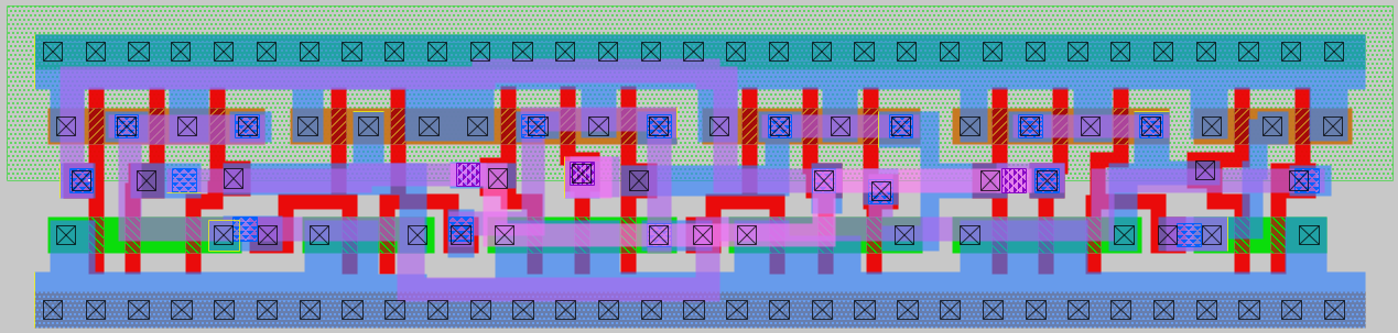
The idea of making this as small as possible already sets many constraints about how things should look like. All the transistor channels have a width of 130 nm and a height of 300 nm, which is the minimum allowed. In standard cell libraries it is common to have some transistors with a larger height, specially if they need to drive a larger fanout. Therefore, the power rails are placed further apart, making the cell taller, Here the separation between the rails is the minimum allowed by all the DRCs regarding separation between diffusion and wells.
I have also made the diffusions for the transistor sources and drains as narrow as possible. This depends on whether there is a diffusion contact and whether there are channels on both sides of the diffusion or only on one, due to the required separation between diffusion contact and channel. There are some exceptions in which I have needed to make some diffusion areas wider to be able to route the polysilicon for the gates, while maintaining the required separation to other gates.
When keeping things this small, probably the largest challenge is to fit the polysilicon contacts, since they take a lot of space. This explains the funny shapes in the polysilicon layer and why there are no two gates that look alike. Routing on the metal layers is also challenging, and I found that I needed to use three metal layers to get everything routed. In contrast, standard cell libraries, which are larger, often can route everything in a single metal layer.
The following shows a comparison of my fdc_dense flip-flop (top) and the IHP-Open-PDK standard library sg13g2_dfrbpq_1 (bottom), imported from the GDS II into magic.
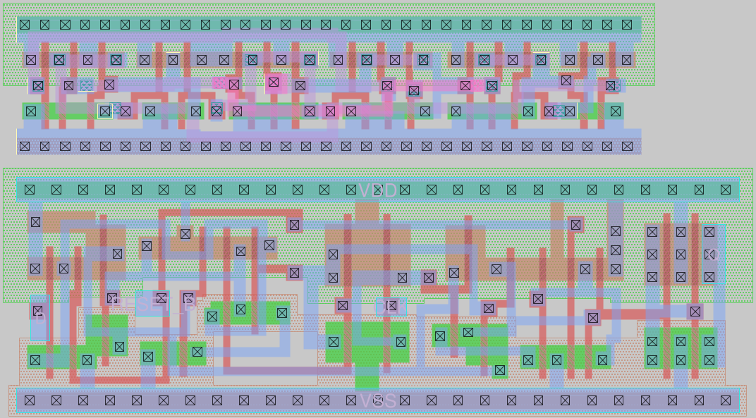
Note that the standard library cell has output transistors that are three contacts tall on the PMOS and two contacts tall on the NMOS in order to properly drive higher fanout loads. My output transistors are just one contact tall and would need a buffer to drive the load unless the fanout is small. It is also clear how the difference in the height of the cells makes routing much easier in the standard cell. In particular, the standard cell uses the polysilicon layer to connect together the gates of multiple transistor pairs, avoiding the need to run metal contacts for these. I simply cannot do this trick with the height I have chosen for my cell.
There is almost a difference in area of a factor of two. My cell is 31.8 μm², while the standard library cell is 59.8 μm². Therefore, I think that trying to make such a small cell was worth the effort and could be interesting to use in some cases.
ngspice simulation and unit testing
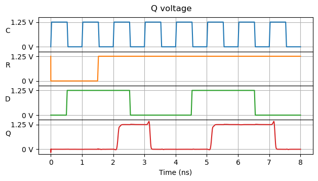
Before measuring the timing properties of the flip-flop it is necessary to do some basic simulations to check that the circuit is indeed working as a flip-flop, and that there are no wiring mistakes. For this, I wrote a simple spice script that generates simple waveforms for the clock, reset and data. The voltage at the output of all the NAND gates, including the Q output of the flip-flop, is output to a text file. This can then be plotted in a Jupyter notebook, and the plots can be checked visually to verify that the cell is working as intended. The following plot shows the three inputs and the Q output. The notebook contains the plots for all the other gates.
Timing simulations
Timing simulations are driven from a Jupyter notebook, which generates a spice file, runs it with ngpsice, and collects and processes the results. This is because I need to run multiple simulations using different transistor models and other parameters, and it is not possible to script all of this in a single spice file.
Output delay
The simplest timing simulation is the output delay simulation. This consists in measuring the time from the clock rising edge until the output Q has its new value. Since the PMOS and NMOS transistors have different performance, it is necessary to measure this both when Q changes from zero to one and when it changes from one to zero. As we will see later, we will need to revisit the output delay measurement when we consider setup time, but for now this is a good exercise to start.
The spice model for low-voltage MOS transistors in the PDK has different libraries, known as corners, which characterize the variability in transistor manufacturing. These corners are:
mos_tt. Typical transistors. All the parameters are deterministic.- mos_tt_mismatch. Typical transistors with mismatch. This is the same as
mos_tt, but thewandlparameters, which define the width and length of the transistor channel, are chosen randomly according to a Gaussian distribution centred on their nominal values. Additionally, thedelvtoandfactuoparameters are also chosen randomly, but I have not investigated what these parameters mean. See the model definition for the relevant formulas. - mos_tt_stat. All the transistor parameters are chosen randomly according to Gaussian distributions. See the relevant formulas.
- mos_ss. Slow NMOS and slow PMOS. The transistor parameters are chosen to get the slowest behaviour possible. Everything is deterministic.
- mos_ss_mismatch. Most parameters are as in
mos_ss, butw,l,delvto,factuoare chosen randomly as inmos_tt_mismatch. - mos_ff. Fast NMOS and fast PMOS. The transistor parameters are chosen to get the fastest behaviour possible. Everything is deterministic.
- mos_ff_mismatch. As
mos_ffbut with randomw,l,delvto,factuo. - mos_sf. Slow NMOS and fast PMOS. Deterministic.
- mos_sf_mismatch. As
mos_sfbut with randomw,l,delvto,factuo. - mos_fs. Fast NMOS and slow PMOS. Deterministic.
- mos_fs_mismatch. As
mos_fsbut with randomw,l,delvto,factuo.
Besides the corner, other parameters that we can vary in the spice simulation are the supply voltage and the temperature. These also affect the timing properties.
Since simulating all the possible combinations of corners, temperatures and voltages is very time consuming, for the output delay simulation I have done the following runs:
- 100 runs of
mos_tt_statwith random supply voltage (nominal 1.2 V, with maximum error ±0.05 V) and random temperature between -10 and 100 ºC). - One run of
mos_ffwith nominal supply voltage (1.2 V) and temperature (27 ºC). - One run of
mos_sswith nominal supply voltage and temperature. - One run of
mos_sfwith nominal supply voltage and temperature. - One run of
mos_fswith nominal supply voltage and temperature. - One run of
mos_ttwith nominal supply voltage and temperature.
These runs give a good idea of what the behaviour of each of the corners are. The output delay simulation results are shown in the plot below. The Q output is coloured depending on the corner used for the corresponding run. mos_ff is shown in red, mos_ss is shown in blue, mos_tt is shown in green, mos_sf and mos_fs are shown in black, and all the mos_tt_stat runs are shown in grey.
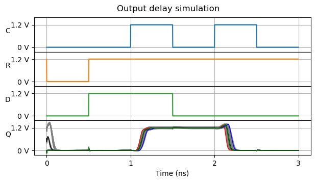
We see that the mos_ff and mos_ss runs indeed give pretty much the fastest and slowest output delays of all runs. There might be some mos_tt_stat runs which are slightly slower or faster, due to the additional effects of supply voltage and temperature. The mos_tt corner gives a delay which is more or less halfway between the slowest and fastest delay. The mos_sf and mos_fs corners also give an intermediate delay.
Now let us think about how to turn the plot above into numbers for a flip-flop datasheet. For static timing analysis we are not only interested in a single number. We need an interval defined by two extreme values, inside which the output transition is guaranteed to happen. These extreme values are:
- Fast corner output delay. The output is guaranteed not to have transitioned before this time in all cases. This value is used, for instance, for hold analysis in the source flip-flop.
- Slow corner output delay. The output is guaranteed to have transitioned after this time in all cases. This value is used, for instance, for setup analysis in the source flip-flop.
Something else we need to define is when to consider that the output is low or that it is high, since the output voltage is a continuous function that takes around 100 ps to slew. For this I will use the common CMOS logic thresholds, in which a low value is defined as anything below 30% of Vdd and a high value is defined as anything above 70% of Vdd. Perhaps it is possible to choose these values more accurately by considering at which voltage an NMOS and a PMOS turn on with this technology, but there is no clear cut, since transistors don’t change abruptly between off and on, and the required gate voltage also depends on process parameters.
The fast output delay is defined as the maximum time such that all simulations have Q still below 30% Vdd for the low to high transition and all simulations have Q still above 70% Vdd for the high to low transition at and before this time. The slow output delay is defined as the minimum time such that all simulations have Q above 70% Vdd for the low to high transition and all simulations have Q below 30% for the high to low transition at and after this time.
With these definitions we can process the simulation traces and obtain a fast output delay of 101 ps and a slow output delay of 229 ps.
Setup
The setup time of a flip-flop is defined as the time, with respect to the rising edge of the clock, such that the input needs to have achieved a stable value at or before this time in order to be correctly captured by the flip-flop. There is a sign convention here which is important to take note of. Usually the setup time is before the clock edge, but this need not be the case, depending on the flip-flop design (just think of a flip-flop that delays internally its clock input more than the data input, either on purpose to optimize timing properties or for architectural reasons because it goes through some buffering). Therefore, many people define a positive setup time to mean a time before the clock edge. However, other people, including Vivado’s timing analysis, define a negative setup time to mean a time before the clock edge. I will use the later convention, as it makes the math simpler and it makes easier to relate setup time and hold time.
A common thinking is that it is important to meet the setup time of a flip-flop because if there is a setup time violation and the input signal changes after the setup time, then the flip-flop may go metastable, which means that its output does not converge reasonably quickly to a low or high value, and takes a long time to settle to a well-defined logic level. That is only partly true. Achieving metastability in a flip-flop is, in a sense, like balancing a pen on its tip. It is technically possible, but it requires a carefully crafted input, and the state is unstable and does not last much because of external perturbations.
The following simulation gives us a better idea of what a typical setup violation looks like. In this simulation, the mos_ss corner is used in all the runs. In each run the transition of the data input is changed, ranging from 100 ps before the clock edge to 10 ps before the clock edge, in 1 ps increments. The D trace and its corresponding Q trace are colour coded.
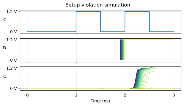
The first thing we notice is that there is no metastability in any of these runs. In all these simulations, the D input slews instantaneously from 0 to Vdd. Maybe I would have gotten metastability if I had played with a slower slew rate.
What we see is that when the data transitions well before the clock, then the output transitions approximately 230 ps after the clock edge, as we had seen in the output delay simulations. However, as the data transition keeps approaching the clock edge, the corresponding output transition happens later and later. At some point it transitions approximately 500 ps after the clock edge. This increase in output delay is non linear. All the D input traces are spaced by 1 ps steps, but clearly the spacing in some of the Q output traces is much larger than that. When the data transition approaches the clock edge even more, the new data is simply not captured and the Q output stays low.
Therefore, we see that rather than the common thinking of “setup timing needs to be met because otherwise the flip-flop might become metastable”, a more accurate thinking would be “setup timing needs to be met because otherwise the flip-flop will exceed its required output delay”.
Exceeding the output delay is bad, because then some paths at the output of this flip-flop will fail setup timing if they did not have sufficient slack, and again this will mean an excessive output delay also for those flip-flops, and this effect will ripple through the system, potentially causing all sorts of misbehaviour.
With this reasoning I am not implying that flip-flops will never go metastable if their setup timing is violated. Something interesting about digital logic is that a typical 100 MHz clock has \(10^8\) rising edges per second. So if the probability that in each data capture the flip-flop goes metastable is \(10^{-9}\) (which would be considered a tiny probability in many other contexts), then on average we will see a metastable state once every ten seconds. It would be quite difficult to hit a situation that has \(10^{-9}\) probability by running randomized spice simulations, but we will see this event happening relatively frequently when running the hardware.
Nevertheless, the main point I want to make here is that the definitions of setup time and output delay are intertwined. Taking into account setup time, we should rewrite the definition of slow corner output delay stated above as follows:
- Slow corner output delay. The output is guaranteed to have transitioned after this time in all cases whenever the input data does not transition at or after the setup time.
We see that keeping the slow output delay as the 229 ps that we measured in the output delay simulation is not reasonable. That would impose a fairly strong restriction on setup time. It would need to be too large (and negative). We might ask: what happens if we increase the output delay definition to 300 ps? That would reduce the setup time (in the sense that it would still be negative, but closer to zero). How about increasing the output delay to 400 ps?
The correct approach to this question is to consider a metric which is the difference of the slow corner output delay minus the setup time. This metric is the thing that matters for the setup timing analysis for a path between two of these flip-flops. In the datapath delay we have the slow corner output delay of the source flip-flop plus other terms. In the destination clock path we have the setup time of the destination flip-flop plus other terms (here is where the sign convention for setup time matters). Since the setup slack is the difference between the destination clock path and the data path, making this metric smaller will increase the slack, which is what we want to have in order to make timing closure easier.
For each setup time, defined as the moment in which the data input transition happens, ranging from -110 ps to -40 ps in 1 ps increments (these are all before the rising edge of the clock), I have simulated 50 runs of the mos_ss_mismatch corner with random supply voltage and temperature, both for a zero to one data transition and for a one to zero data transition. For each setup I measure the largest output delay of all the corresponding simulations, and then plot the cost metric (output delay minus setup) with respect to setup time.
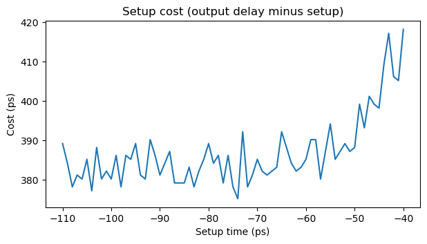
What we see is that as the setup time gets closer to zero, the cost increases non linearly. However, for a certain range of setup times the cost metric is rather flat and small. If we extended the plot to the left, to more negative setup times, we would see the metric increasing again. Since we want to minimize the setup cost metric but also make the setup time as small (close to zero) as possible (the reason for this will be more clear when we think about hold timing), from looking at the plot we see that it is reasonable to define the setup time as -70 ps. A conservative cost for this setup time would be 395 ps. This implies that the output delay should be defined as 325 ps.
These considerations regarding the relation between setup time and output delay also show that the typical method of doing static timing analysis per path can be too pessimistic in some situations. For instance consider three flip-flops connected through some logic as F1 🡒 F2 🡒 F3. Assume that the path from F1 to F2 is rather short, so the data arrives to F2 well before the clock rising edge. Therefore, we know that the in the worst case the output will be available 230 ps after the clock rising edge, since that is the output delay we have measured for the case when the data arrives early enough to the D input. However, the static timing analysis of the path F2 🡒 F3 must use 325 ps as the output delay of F2, since the analysis does not know by only looking at this path how early the input data will arrive to the D pin of F2.
Hold
The hold time of a flip-flop is defined as the time with respect to the clock rising edge such that the input must not change at or before this time. In this sense, the setup time and hold time define a time window with respect to the clock edge that is the capture window of the flip-flop: the data input must be stable during this window in order for the flip-flop to work properly.
There is also a sign convention associated with hold time. In this post I will use the convention where a positive hold time means after the clock edge. This is the most common convention, but note that some flip-flops can have negative hold time with this convention. This simplify means that the capture window of the flip-flop happens strictly before the clock edge. This is a point that Matt Venn makes in his video. A flip-flop with negative hold time, and more generally a flip-flop whose hold time is less than the fast corner output delay, cannot violate hold except if there is clock skew.
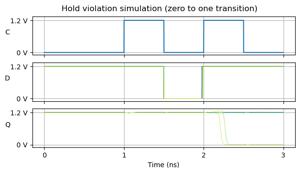
The following simulation gives us a good idea of how hold violations work. Here the situation is that the input data of the flip-flop is zero, but it is going to transition near the clock edge. We expect the output of the flip-flop to be zero in the next clock cycle. If the output goes to one, then it is because hold was violated. The transition times range between -25 and -15 ps, spaced in 1 ps intervals.
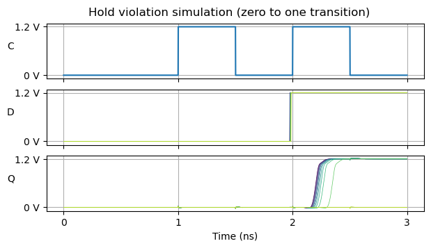
We immediately see that this simulation looks very much like the setup simulation that we have done in the previous section. Ultimately we are simulating the same thing: a data change that happens near the clock rising edge. However, we look at different things in the output in each case. Also, this simulation is done for the mos_ff corner, since the worst case for hold time happens when the transistors are fast.
We can see that in a few of these cases (all of which transition at or before -15 ps), the flip-flop output stays at zero. This means that for the zero to one transition the hold time of this flip-flop is negative. The input data is allowed to change slightly before the clock edge, and the flip-flop will still correctly capture the previous value.
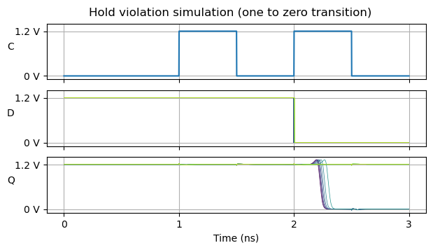
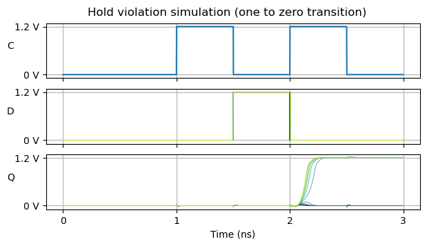
If we do a similar simulation for the one to zero transition, we see that the flip-flop has a different hold time for this transition. In this case the time when the input transition happens ranges from -5 ps to 5 ps with respect to the clock edge, in 1 ps steps.
In order to obtain a hold time for the flip-flop datasheet, we need to consider the worst case, which is the greatest (more positive) value among all the ones we have seen.
There is another pattern for the data input that is relevant for the hold simulation. This is illustrated by the following plot. It considers the case in which the flip-flop output has the value one, and the input is zero, but transitions to one near the clock edge. In this case we expect that the flip-flop output transitions to zero some time after the clock rising edge. If this doesn’t happen, then it is because hold was violated. Comparing this to the simulation above for which the input transitions from zero to one (so the Q output must remain all the time at zero if hold is met), we see that the range of transition times for which hold is met is similar, but not exactly the same.
The complementary case is that in which the flip-flop output is zero, the input is set to one, but transitions back to zero near the clock rising edge. In this case we expect that the flip-flop output transitions to one.
To do a more complete hold simulation, I have done 250 runs of the mos_ff_mismatch corner with random supply voltage and temperature, with the data transition happening at times between 5 ps and 10 ps with respect to the clock rising edge in 1 ps steps. In each case I am testing the 4 different input cases that have been shown above. A transition time is set to meet hold if for all the 250 runs for that transition the flip-flop output is at the value that it should at and after some time after the clock edge. The smallest (most negative) time for which hold is always met is 9 ps. Therefore, this is the hold time for the datasheet of the flip-flop.
Summary
According to the discussion above, the datasheet for this flip-flop could list the following values:
- Setup: -70 ps
- Hold: 9 ps
- Output delay: 325 ps
In this analysis I have simplified some things. A real datasheet for an ASIC cell, such as the ones in the standard library of this PDK would consider different cases of output load capacitances and slew rates for the input signals, while in this analysis I have considered no output load and zero slew rate for inputs.
Additionally, there are other timing properties related to the asynchronous reset input that I have not analysed. These are:
- How much time before the rising edge of the clock the reset needs to be deasserted to guarantee that a one at the input is correctly captured.
- How much time does a reset pulse need to last to guarantee that the flip-flop is successfully reset.
Finally, to really have confidence that the above timing requirements can be safely used in any situation, it might be worth to simulate some corner cases. For instance, if the data input is zero except during the capture window between the setup and the hold times, where it is one, is a one correctly captured by the flip-flop always?
Conclusions
In this post I have shown how an ASIC flip-flop can be designed in Magic and simulated with ngspice. I have considered the timing analysis for the output delay, setup and hold of the flip-flop. I show that setup time and output delay are related and should be defined together. Regarding setup time, a mental model that is useful to have in mind is that if the input of a flip-flop violates the setup time, then the output delay could be more than what the datasheet says, thus potentially causing a cascade of timing problems throughout the design. This idea is more accurate than the common mental modal that says that if the input violates the setup time then the flip-flop might go metastable.
All the code and design files used in this post are contained in the flip-flop-timing repository.
I did these experiments in Cadence Virtuoso for my masters